2016-04-14 18:51:21 chip
Page 1662
📢 PUBLIC
April 14 2016
The schematic is nearly finished. I still need to sort out how I
will handle power selection -- probably just with header pins for the
first version. I double-checked the BOM spreadsheet, making sure every
component had a PartID.
I need to make sure every part has a land pattern before I can
begin laying out the board. This is another tedious task. It isn't
difficult and each individual part doesn't take more than a few
minutes, but it is extremely detail-oriented and easy to make
mistakes. This is also where I refine the BOM and update the project
library components to include the information for exactly the part
that is being used. When I am done, all the components used in the
schematic should reference only the project-specific library.
The part name in the BOM should be a combination of the DipTrace
component name and the Autotronik name. For example:
MSP430F5529-LQFP80
TPD2E-SOT553
The first part of the name lets me quickly find the component in
DipTrace. The second part lets me quickly find the component in the
Autotronik PnP component library. The two names are not equivalent!
The PnP machine only cares about the shape of the component, all
LQFP80 components are the same, all 0402 resistors use the same
component definition. DipTrace needs to know the exact component,
including its pin assignments and values.
The most methodical approach is to start with the BOM parts list.
For each PartID:
- Find the first RefDes. For example, PartID 1 is U201.
- Go to the schematic and look up the component name by its RefDes.
U201 is "LQFP80 - MSP430F5529".
- Go to the component editor, make sure the project library (CtrlMtr01)
is selected, and select the component "MSP430F5529".
- Click on "Pattern" in the properties and verify the correct
land pattern is shown.
- If there is no pattern or it is the wrong pattern, I need to
create the pattern and assign it to the component.
To create a new pattern:
- Open the pattern editor and make sure the project library is
selected.
- If this is a standard pattern such as 0402 or 0603 I can copy
the pattern from the stock library.
- To create a new pattern, I first need to look up the pattern
in the component datasheet.
The easiest way to do this is to look up the part by its VendorID
(from the BOM) and then enter the VendorID on the vendor's website
(Digikey). The component info should include a link to the
manufacturer's datasheet. For complicated components like an MSP430,
I need to be careful to pay attention to the full part name. In this
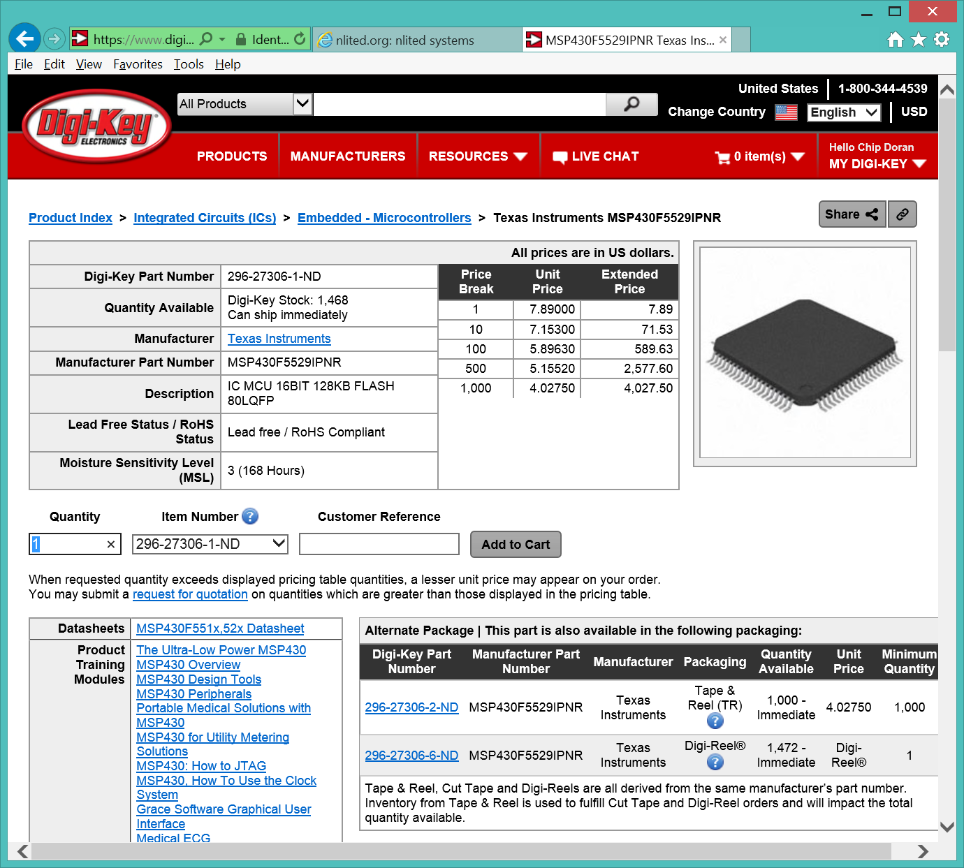
case I need the land pattern for the MSP430F5529IPNR.
For example:
U201 > PartID 1 > Vendor=Digikey/296-27306-1-ND
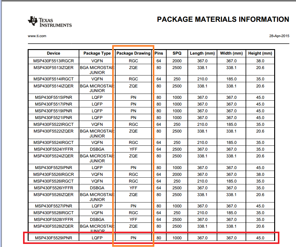
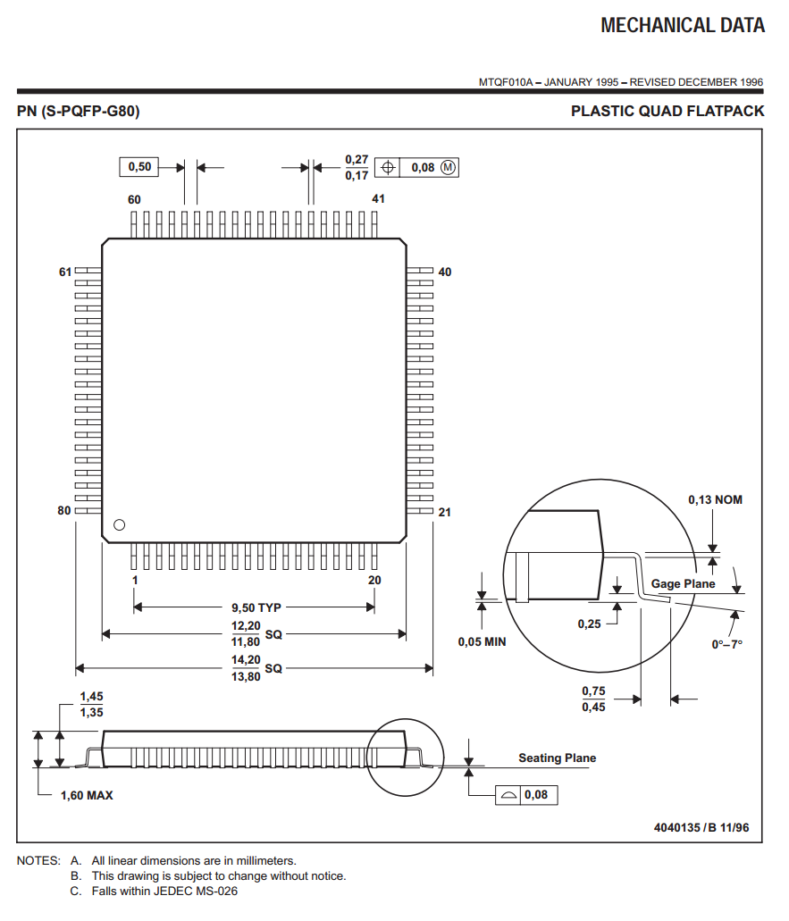
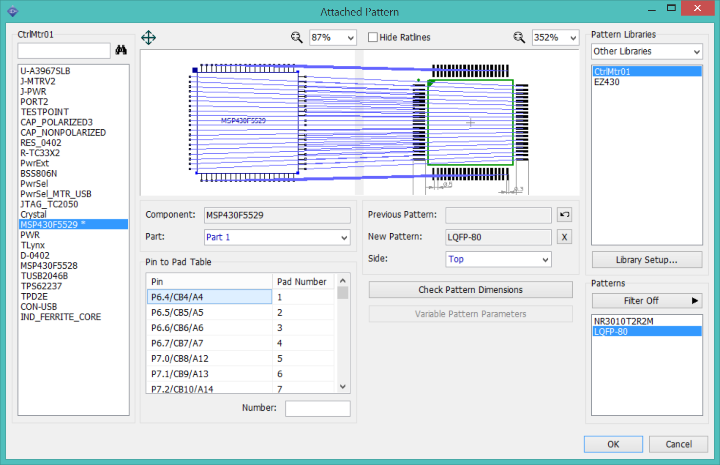
The LQFP-80 is a 14x14mm die with a 0.5mm pin pitch. This is the
stock DipTrace pattern "QFP-80/14x14x0.5". I measure the pattern to
make sure the pads are slightly larger than the pins. I copy the
pattern to the project library, rename it LQFP-80 to match the
name of the MSP430 part, and save the CtrlMtr01 library (not
the standard pattern library). Now I can go back to the MSP430F5529
component's attached pattern window, click on the CtrlMtr01 pattern
library to refresh, and select the "LQFP-80" pattern. The pins should
magically attach themselves. Verify in the datasheet that pin 1 is
actually P6.4.
I forgot to apply custom paste shrink to the pads, and the first
build resulted in far too much solder and catastrophic bridging. Every
pad should have a paste shrink value, with large pads having
significant shrink values. See .
Create an additional field named "Library" and set it to the
pattern library name. This will be very helpful when copying the
pattern into other libraries later.
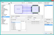
Click OK to save the pattern, then save the component library.
Go to the schematic editor, right-click the component and select
"Update from library..." > "Similar Name Components". Now I should
be able to right-click the component, select "Properties" >
"Attached Pattern..." and see the new pattern.
NOTE: Updating the component will lose any changes made
to that particular instance of the component, such as which pin
names are shown. Don't bother setting the pin visibility until
the schematic and component selection is final.
Updating a pattern for an existing component:
- Update and save the revised pattern in the pattern library.
- Open the component library, select the component, click Pattern...
and select the new pattern from the library. This needs to be done
even if the referenced pattern is the same; the component library
keeps an internal copy of the pattern that needs to be updated.
Save the component library.
- Open the schematic, select an instance of the component, and
select "Update from library... Similar named components". Save the
schematic.
- Open the layout, renew from the related schematic.
- Select an instance of the component in the layout and select
"Update from library... Similar named component". This extra step is
necessary to update the shrink/swell attributes.
- Export the TopMask, TopPaste, and Top gerbers.
- Launch GerberLogix and load the gerbers, then verify that the
pattern changes are present.
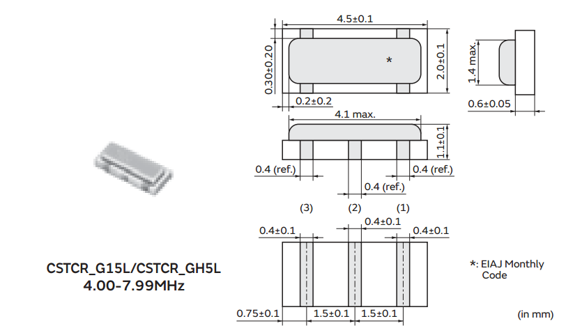
I found an error: I had Q204,Q101 marked as a 6MHz crystal (Digikey
490-1204-1-ND) when the LaunchPad uses 4MHz (Murata CSTCR4M00G15L99,
Digikey 490-7861-1-ND). Then I have Q401 as 4MHz when it should be 6MHz.
{THREAD_LINK:1434} I need to double-check that pin 1 and pad 1 are
properly connected; the datasheet for the fixture doesn't concern itself
with actual pin assignments.
=====
April 15 2016
22:00> The component patterns are complete, time to begin the initial
layout!
22:40> Premature declaration of victory... All the caps were
symbols without patterns. I had to create components for polarized and
non-polarized 0402, 0603, and 1206 caps and then replace all the
components with the new ones. I need to verify the cap sizes.
I am still missing one pattern for the switches. I plan to just use
header pins and jumpers, so I need to replace the switch components
with 2-pin headers.
May 25 2016
The first layout used too much solder paste and failed due to
bridging and pieces that floated onto a single pad. I applied paste
shrink to all the patterns in the project to reduce the amount of
paste applied to the pads. The holes for the header posts were reduced
from 0.040" to 0.035".
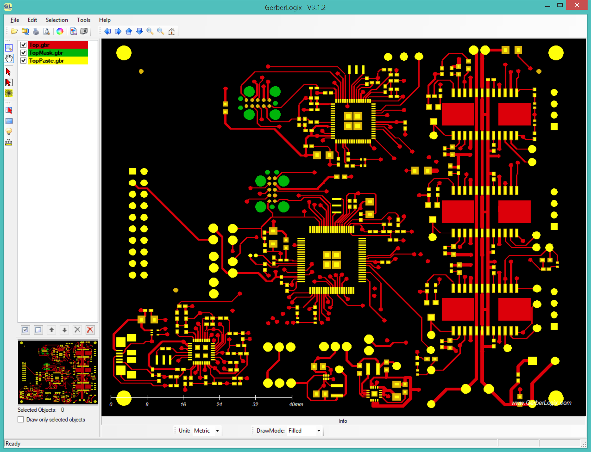
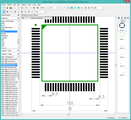
The revised CtrlMtr02 layout with minimal paste areas:
My concern now is that the paste area may be too small to catch the
components during placement, especially the 0603 and 0805 caps and
resistors.
Once I have a working build, I need to migrate all the components
and patterns from the CtrlMtr libraries into the EZ430 libraries to
use for all future projects, then down into the CANMtr libraries.
WebV7 (C)2018 nlited | Rendered by tikope in 102.601ms | 216.73.216.220