May 11 2016
09:30> With the CtrlMtr02.1 project imported into PnP, I have another decision. I can continue to build the paper board and prove the machine can place everything before ordering the boards tomorrow, or I can assume the PnP will work and order the boards today. There is actually very little to learn in building the paper board, the layout is nearly identical to the previous version except that the USB connector has moved a tiny bit. The real change was renaming the components and moving the origin, both of which were effectively tested by importing the new layout.
Placing the PCB order is always a nervous moment; once the order is placed, nothing on the board can be changed. If I discover an error, the time and money spent on the boards is wasted. On the other hand, I need to place the order at some point. My plan for today is to print the new board, carefully examine it -- especially the power selector wiring -- and place the PCB order before noon today and order the stencil tomorrow. The boards should arrive on Monday or Tuesday of next week, by then I should have already received the stencil and the last of the Digikey parts and be ready to build the actual board.
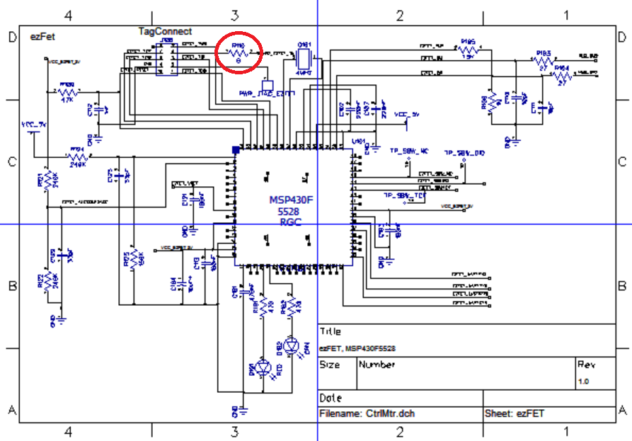
The power configuration FET1, where the board is being powered by the programming tool through the MSP430F5529 JTAG interface, has the JTAG VCC_TOOL ultimately connected back to the JTAG:VCC_TARGET pin. I'm not sure this is correct. VCC_TOOL is an output and VCC_TARGET is a voltage sensing input, but it might be that if the FET senses voltage on VCC_TARGET it may disable VCC_TOOL. This would result in the FET oscillating between ON and OFF. As I am not sure of the behavior, it would be prudent to add a 0-ohm resistor inline with the VCC_TARGET trace. This gives me a quick fix if there is a problem, just pop out (or don't populate) the shunt. I can then replace the shunt with a jumper in the next revision. The same thing applies to the MSP430F5528.
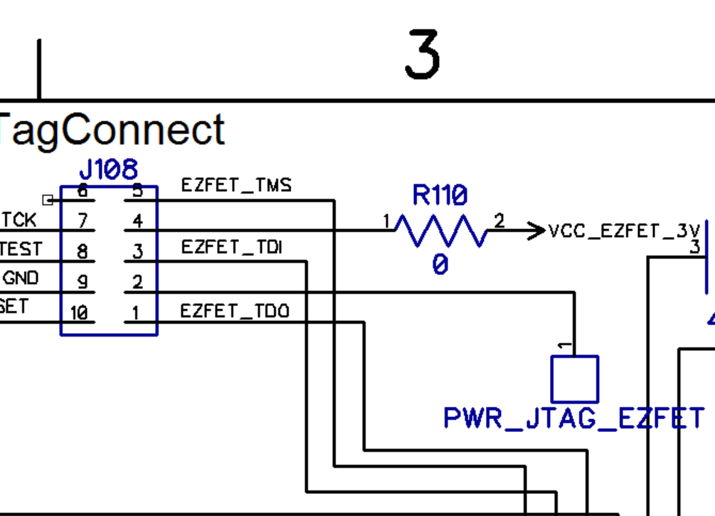
On the ezFET sheet, I insert a 0-ohm 0603 resistor between TagConnect pin 4 (Vcc/Ext) and the VCC_EZFET_3V net.
On the Control sheet, I insert a 0-ohm 0603 resistor inline on TagConnect pin 4 and the VCC_CTRL_3V net.


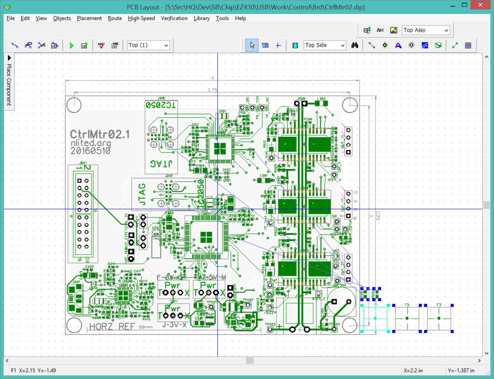
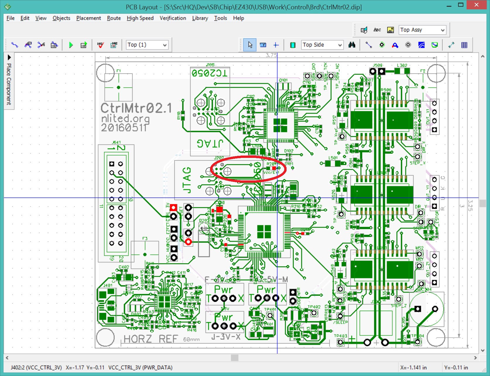
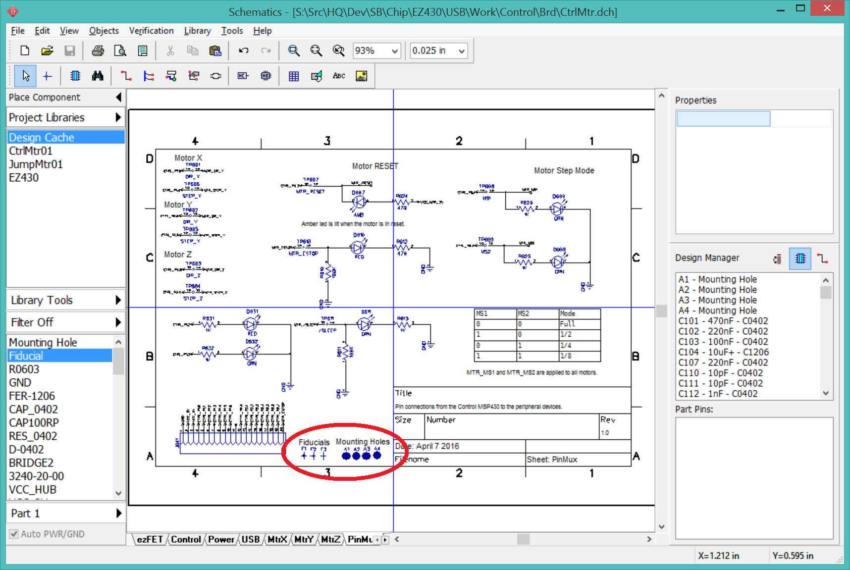
I save the schematic and renew the layout. I tired of recreating the fiducials, so I created a "Fiducial" component and placed 3 of them on the PinMux sheet. They are not connected to anything, this may cause problems or warnings. This seemed to work, the two 0-ohm resistors appeared along with 3 fiducial marks. I placed the 5528 resistor and the 3 fiducials. As I placed the 5529 resistor, I found that DipTrace had connected both ends of the resistor to the same net, VCC_CTRL_3V. I went back and fixed this by deleting the wire between pin 4 and the resistor, recreating it, setting the net class to PWR_DATA, and renewing the layout from schematic again. This time my fiducials survived, no more recreating them every time! When everything is working properly, I can renew the layout from schematic without losing any layout features. Tweaking the layout should be avoided, only used to fix problems in a specific revision after boards have already been fabricated. (Such as fixing problems in the stencil that don't affect the board.)
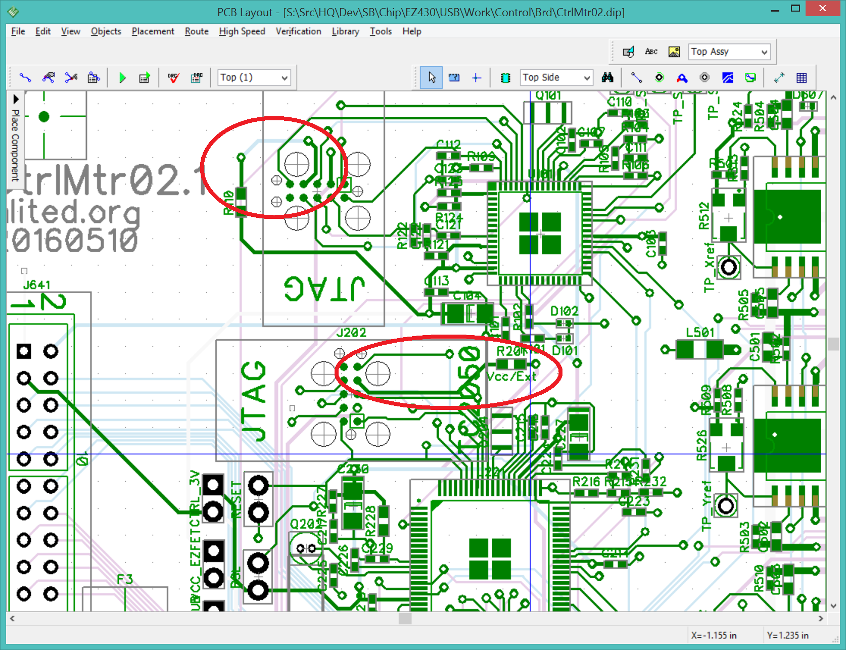
The 0-ohm resistor now isolates the JTAG Vcc/Ext pin from the CTRL_3V net (highlighted). If there is a problem driving the MSP430 without external power (modes FET1 and FET2) I can now pop off the 0-ohm resistor to see if that fixes the problem. If there is a problem and removing the resistor fixes it, then I will replace the resistor with another power selector jumper.
This added 2 new places (of an existing pick) to the PnP file. Hopefully the time spent cleaning up the component names will pay off with a speedy update...
The fiducials are now persistent, so I try to do the same thing with the mounting holes.
I review the gerbers for each layer, making sure the mounting holes are present. I will need to manually trim the mounting holes from the paste layer when ordering the stencil.
Minimizing the number of drill hole sizes helps. I notice some oddball hole sizes:
These changes would reduce the hole sizes from 11 to 6: 0.017 (vias), 0.035 (motor outputs), 0.040 (header pins), 0.051 (terminal block), 0.093 (TagConnect clips), and 0.130 (mounting holes). UPDATE 20160524: This hole exercise was pointless. I spoke with BAC and was told they don't care how many different sizes are present, and they will automatically bump holes to the available drill sizes. I am free to specify as many oddball hole sizes as I want, it won't affect the cost.
15:11> This turned out to be a significant task, especially updating the BRIDGE2 components masquerading as test points. The hole count is now reduced to 6 sizes.
15:40> A review of the gerbers for each layer looks OK. It is too late to submit the PCB order today, I can take the rest of the day to put the order together and submit it first thing tomorrow morning.
The paper board has been built and the final tweaks have been made to the layout. It is time to order the actual PCB's and stencil. I need to carefully review everything; the design is locked in once the boards are ordered, any change after this means throwing the boards away.

I wasn't careful enough! I forgot to shrink the paste apertures.
My shopping list:
I need to archive the state of the design when the boards are ordered, so I create a subdirectory 20160511 that will hold zipfiles of all the source files used for the order. I create a zip\ folder that will hold the files being zipped up.
I copy all the source files for the project into zip, and zip them into an Archive.zip file in the order directory. These files include:
I export the Gerber X2 and N/C Drill files to the zip directory. I include all the layers, even though all the bottom layers are empty. The files are zipped into a BAC.zip zipfile in the order directory.
This is a 4 layer board and will be ordered using Bay Area Circuit's "4 Layer Special" bundle for $180 plus tax and shipping. 4 layer boards are twice as expensive as 2 layer boards.
I pulled the trigger at 08:50 Thursday May 12. The $180 4-layer bundle is $195 after tax and shipping. The shipping charge is $15, which seems especially outrageous as it is being shipped about 20 miles. Order #4183 from Bay Area Circuits.
I don't want the mounting holes to be in the stencil, if they are present they will catch solder paste can create a mess. As through holes, they are present in every layer. And since the stencil uses the soldermask layer, and the mounting holes need to be present in the soldermask, the holes will be included in the stencil. I open the layout, delete the 4 mounting holes, export the Gerber for the Top Paste layer to the zip directory, then close layout without saving the changes. The Stencil file is then zipped into order\Stencil.zip. This needs to be done for every stencil order.
The stencil is ordered after the PCB order has been accepted. OHaraRP.com usually ships a klapton stencil within a day after receiving the order, and the stencil typically arrives before the PCBs.
The stencil arrived on Friday.
May 19 2016
The boards were scheduled to ship today, Thursday, ship via UPS ground and arrive Monday. I changed the order to will-call so I would be able to work on them before the weekend with the hope of having working boards by Sunday afternoon. The trip to Fremont and back took about 1:45 hours, it is now just after noon on Thursday and I have the boards in hand. I am waiting on the stencil to arrive tomorrow.
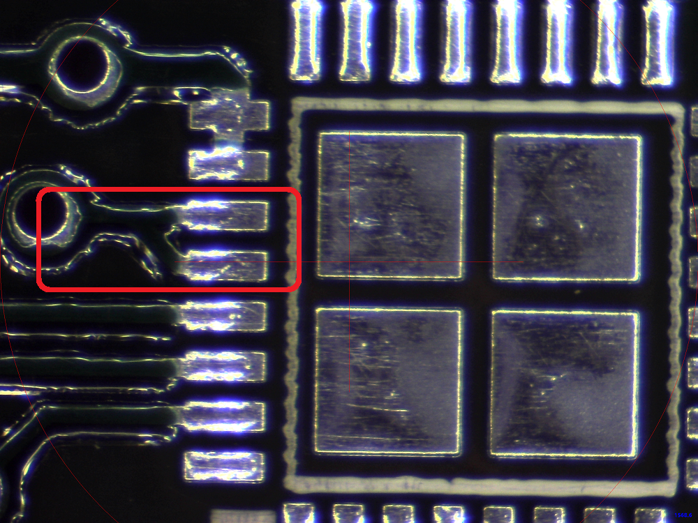
I was concerned about the tiny power converter. It may be an outsized view of the power of electricity, but I have trouble imagining all the power for the entire board flowing through such a tiny (4x4mm) component.
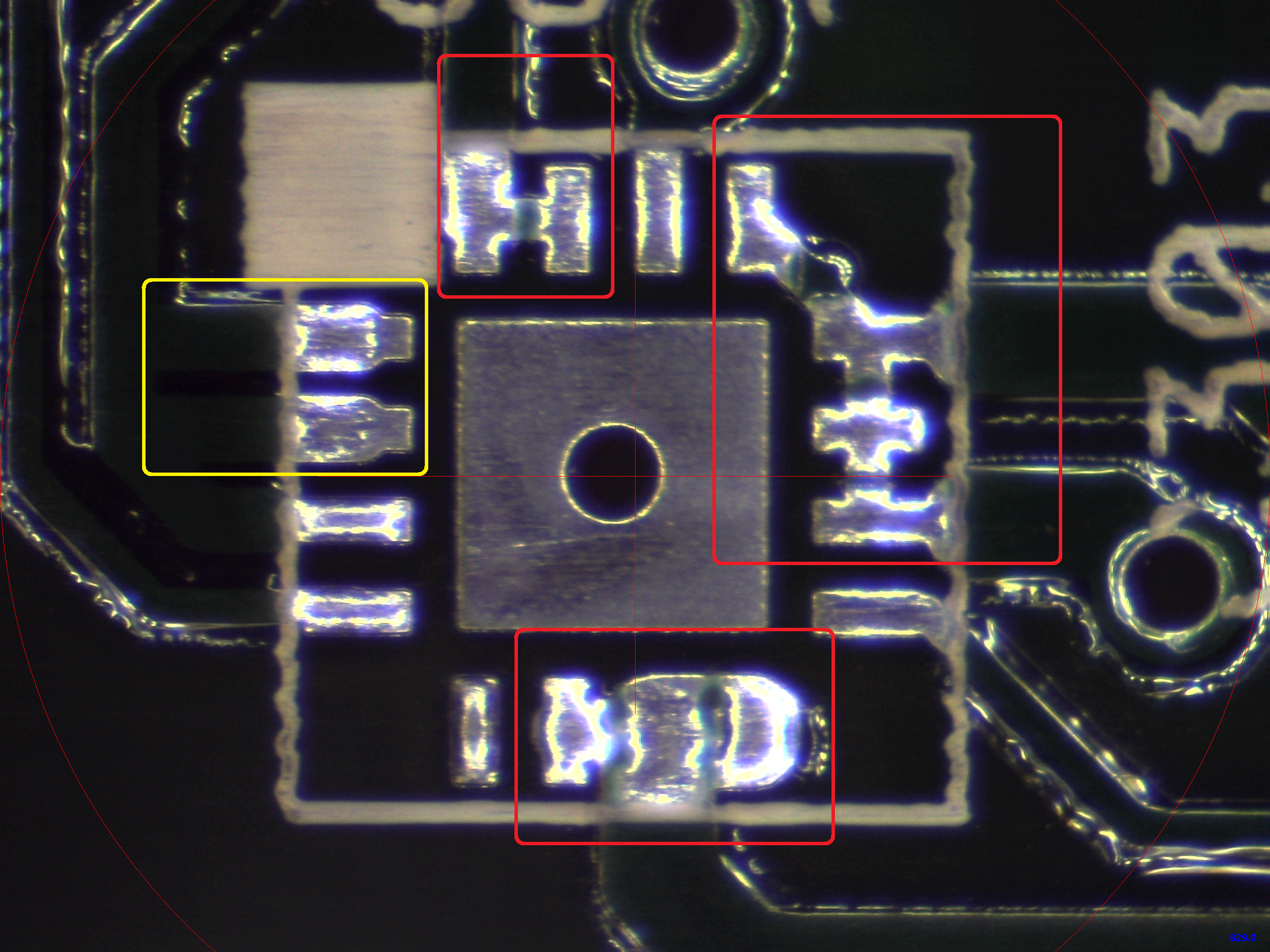
The pads outlined in red are all intentionally bridged. The yellow outlines pads that are not bridged but are joined to PWR_MOTOR traces (0.025"). Running traces directly between the pads causes a lot of distortion in the solder, which could cause a problem during reflow. It would be better to run the traces away from the pads and under the solder mask before joining them together. Running the traces out from the pads at the same width as the pad (0.28mm) and under the mask before widening to 0.025" would remove the distortion from the pads outlined in yellow.
The photo on the right shows the TUSB2046B, which has the same pad pitch (0.5mm) on a slight larger package. This also has two pins bridged together, but here the traces run under the mask before joining and the result is much cleaner with no distortion of the pads or solder piles.
I don't think it is a good practice to have a trace enter a pad from the side. This creates a small solder pile in the middle of the pad where the solder from the trace overlays the width of the pad. The pile is not visible in the photo but it clearly seen when viewed at an oblique angle.
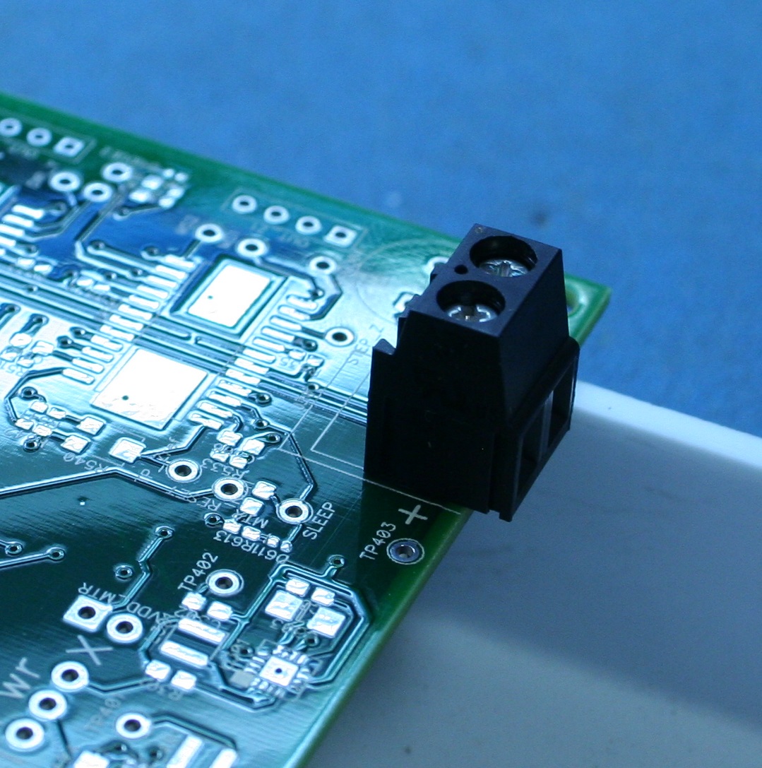
The terminal blocks don't fit correctly, the pattern does not match the actual part. This is not fatal, the terminals should still work but will hang over the edge of the board.
The preflight check is to run Production > Vision Before Production. This will run through the place list with Camera A, providing a view of where each component will be placed.
Markings on the assembly layers won't be printed onto the board.
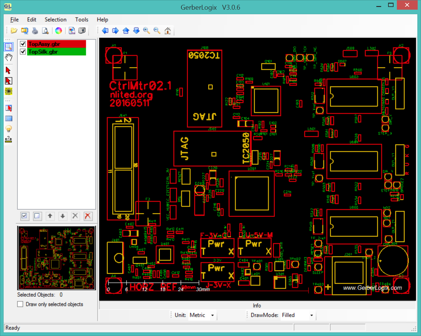
The board is missing the HORZ REF line; I must have either forgotten to add it or added it later. No, all my assembly layer markings are missing. I spoke with BAC engineering support, who explained that the assembly layer is used only for notes and is not printed onto the board. Only the silk layers are printed. In this case, the component outlines were present in both the silk and TopAssy layers while my text was only in the TopAssy -- which was not printed and my text was dropped. Lesson learned: Only the silk layers are printed onto the board.
This gerber view shows the TopAssy in red, TopSilk in green, and anything in yellow is present in both layers.
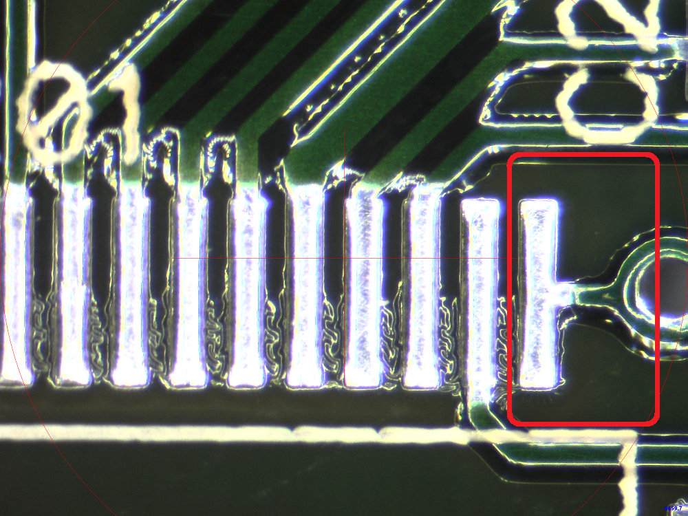
Is D607 the right size? The component outline is 0603 and the pad is 0402. This is the D0603-AMB amber led, which is definitely an 0603 part. The layout has the wrong pattern, the LED0402 pattern is attached to the D0603 component. This is not a fatal error, an 0603 led will sit on an 0402 pad with just a bit less solder, although I need to update the D0603 component to fix this for future boards.
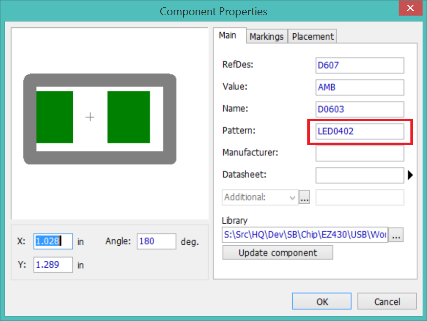
UPDATE: The fit is a bit tight. I will proceed with the 0603 but if it causes problems I can replace it with a red 0402 led in the PnP project.
This is a good time to remind myself how important it is to archive everything every time I place a board order. If I update the component library to fix the D0603 part, I will no longer be able to regenerate the same PnP file for the boards I ordered on 5/12. If, at some later date, I wanted to build out any remaining 5/12 boards I would need to load the PnP file from the archive, not try to regenerate it.
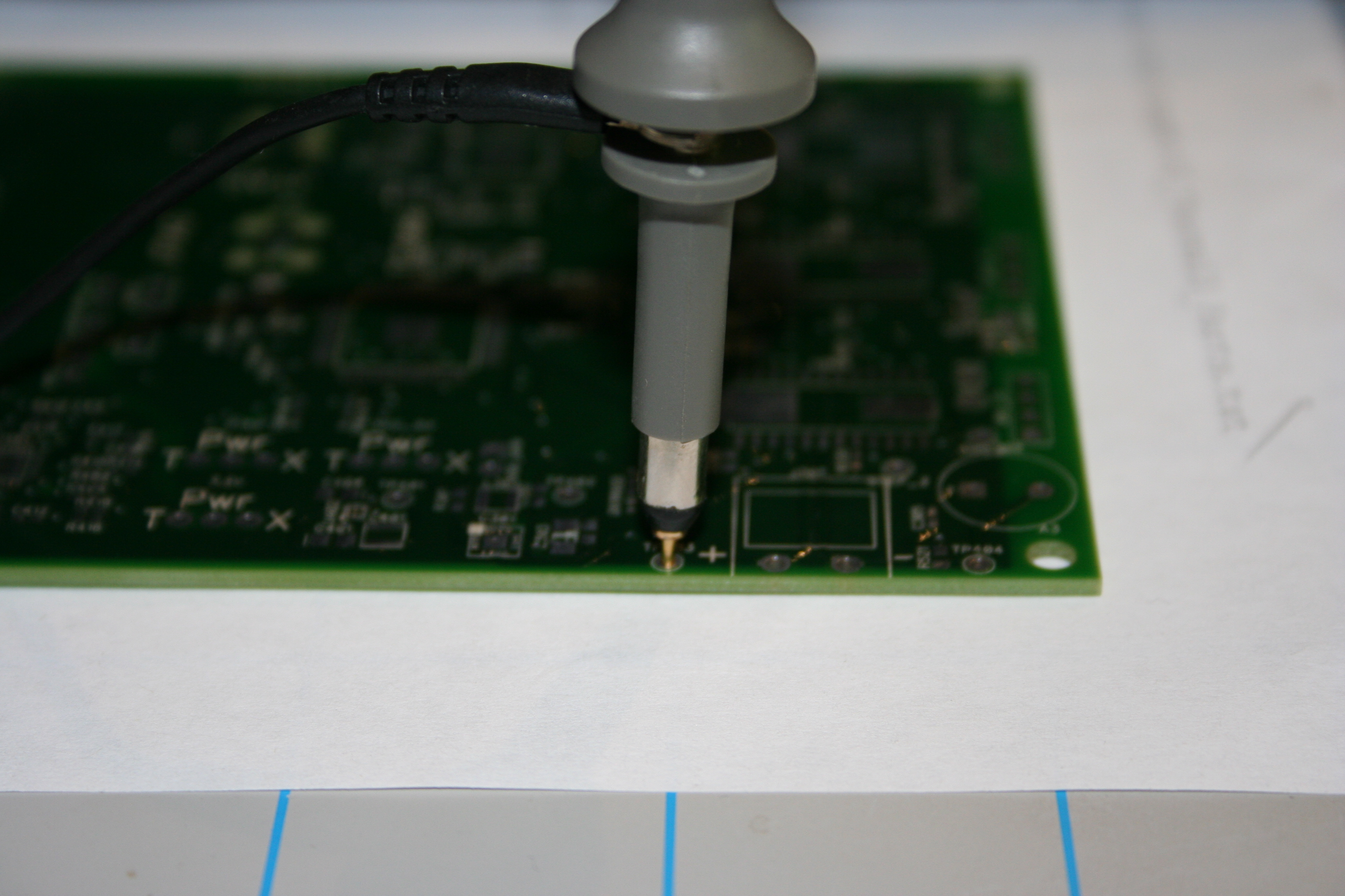
The test points are just the right size to hold the tip of the scope probes.