2016-04-03 20:15:00 chip
Page 1629
📢 PUBLIC
April 3 2016
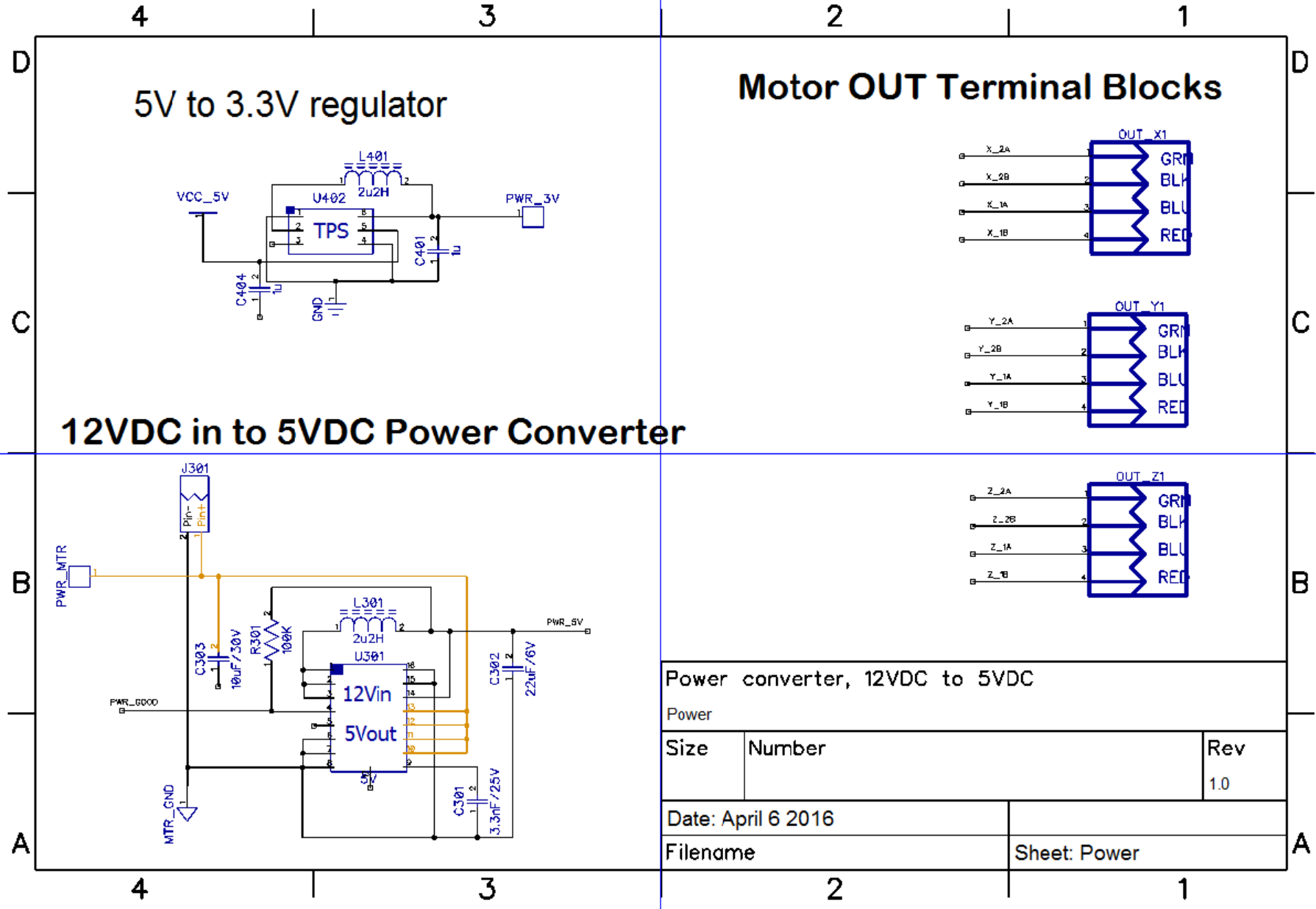
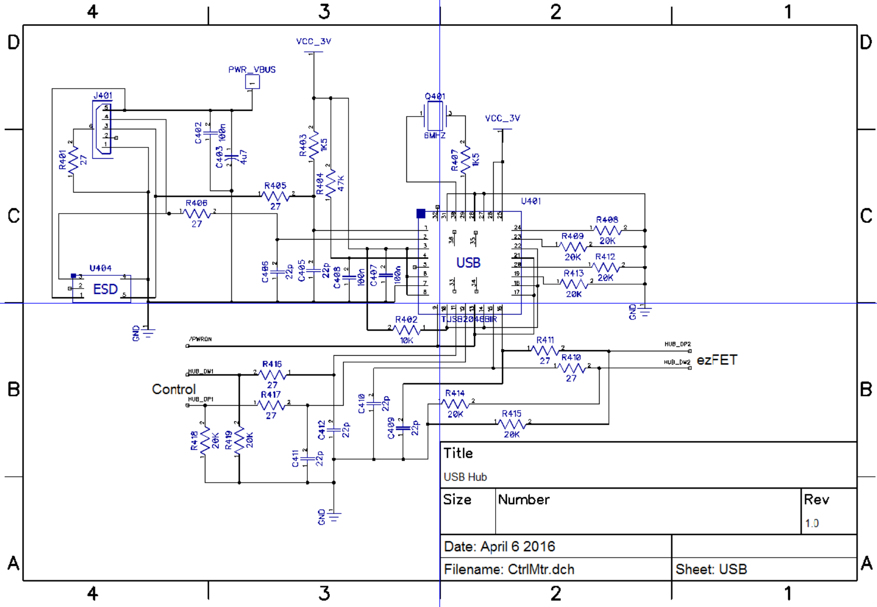
I have collected all the pieces of the puzzle, now it is time to begin
connecting them together: Control, Power, USB, Expansion, and Motor.
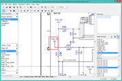
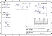
Schematic capture is the process where I create the sketches that describe
how all the components are wired together. The schematic describes the
components only terms of their logical function, there is little or no
concern about physical size or space. Wires can cross over any number of
other wires and reach any component.
As I placed each component into the schematic, I add it to the
Parts list in the AutoBOM. I don't need
to specify the exact part yet, I can leave the component name, value,
and part number blank; I just need to enter the RefDes to create a new
row in the Parts list that will be filled in later. The schematic at
this point is a sketch of the final design, I don't want to be bogged
down in the minutia of looking up datasheets, the goal is to chunk in
the functional blocks quickly, to discover any major design obstacles
as early as possible.
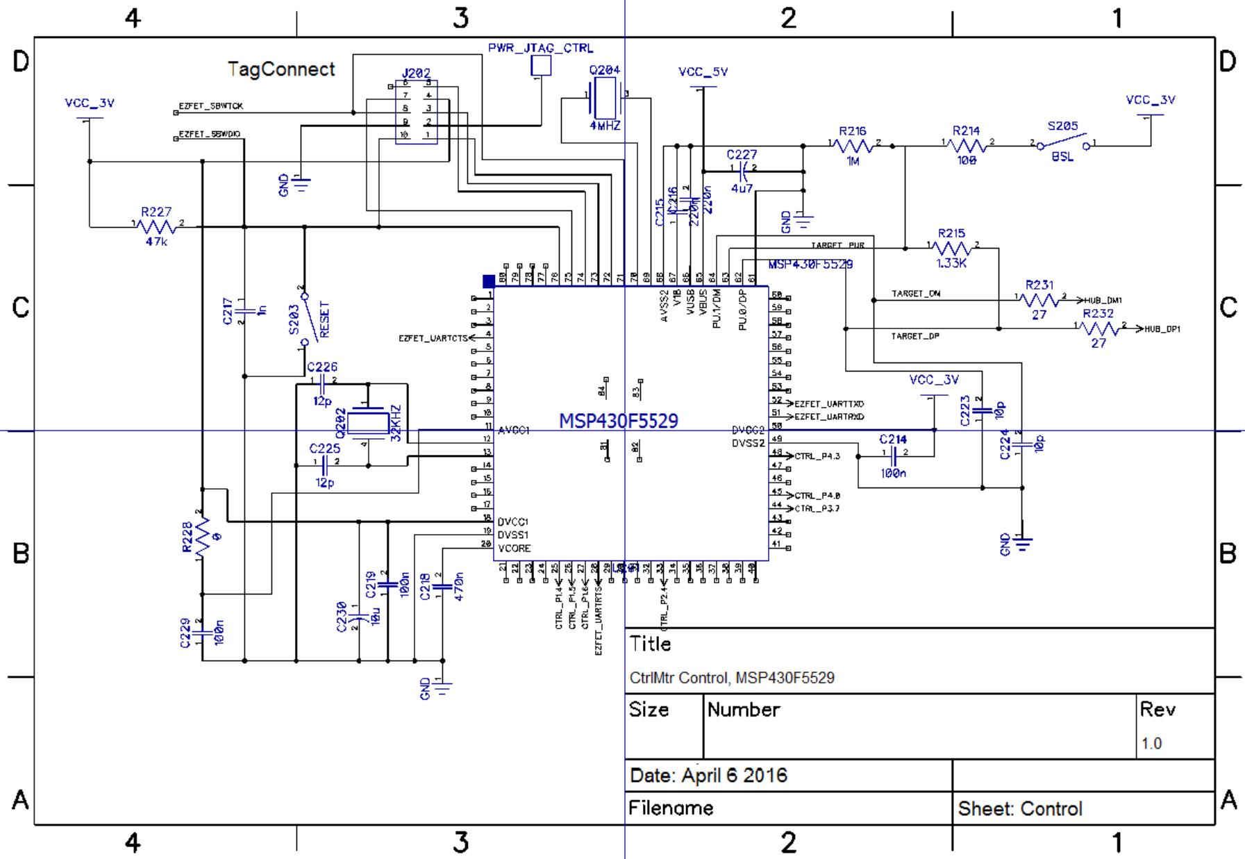
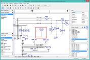
Sheets should be 8.5x11" standard letter size.
When creating multi-page schematics, it is very helpful to
include the sheet number in the component ID. For example, "R104"
is a resistor on sheet 4.
Using "wireless" connections between pins removes the rats' nest
from the schematics and makes off-page connections without requiring
an extra port component.
The component symbol should match its physical pin layout as much as
possible.
Sheets should be letter size. The biggest reason is that when
debugging a circuit, I want to have a hardcopy for notes and easy
reference. Since I don't have a 17x22" printer, a C-sized sheet will
be reduced down to fit onto a 8.5x11" sheet anyway, with an end result
of an unreadable sheet. The second reason is that it forces each
individual sheet to remain simple, with only a single IC. This is a
good thing.
This page
goes into a more detail about the pro's and con's of sheet sizes.
It may be tempting to rearrange the pins on the schematic symbol
for a component to tidy up the schematic. DON'T DO IT. The closer the
symbol matches that actual part, the easier it will be to arrange the
components on the board during the first layout, and makes tracing the
from schematic from the layout much easier.
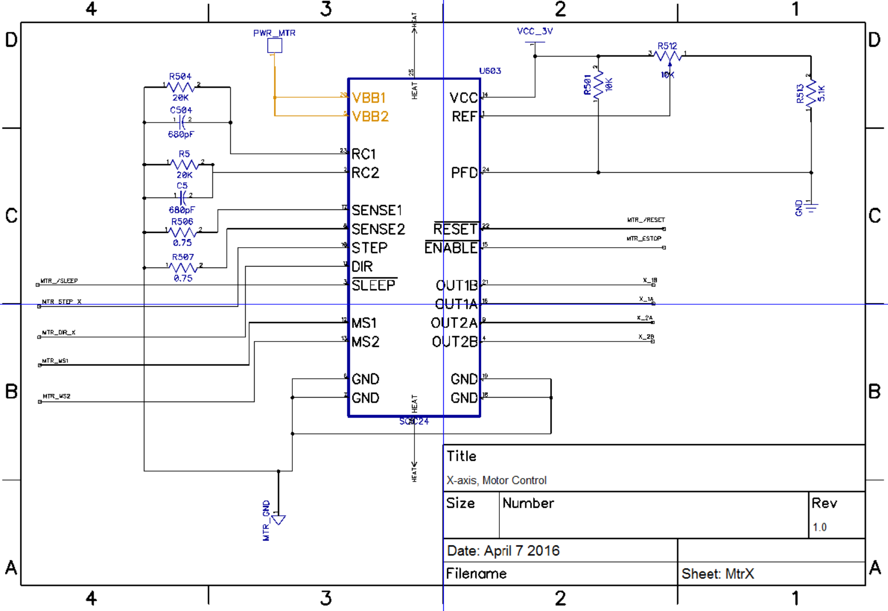
April 18 2016
The first pass at the layout exposed some significant problems with
the schematic. This was not a good thing, but it was also not
surprising. I try not to spend much time trying to make a perfect
layout during the first pass, there is a good chance I will find
problems with the schematic that will trash the layout.
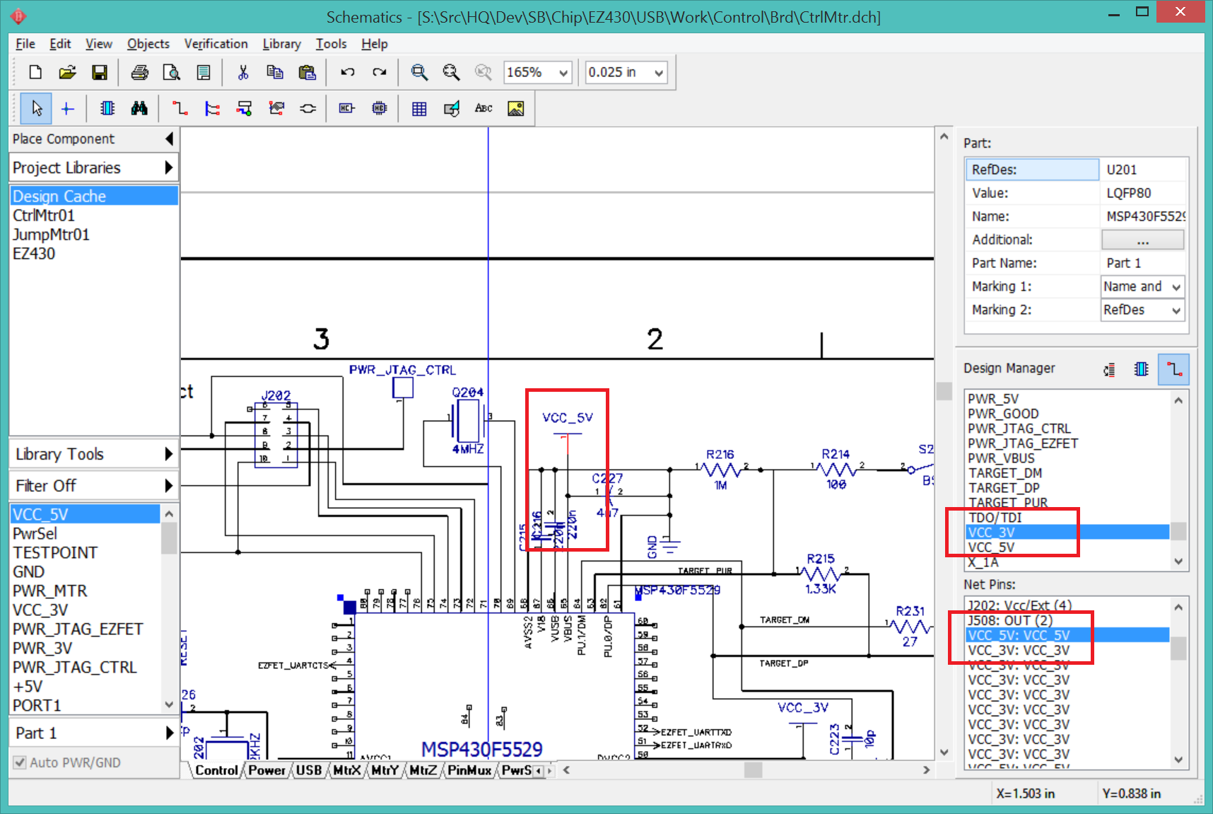
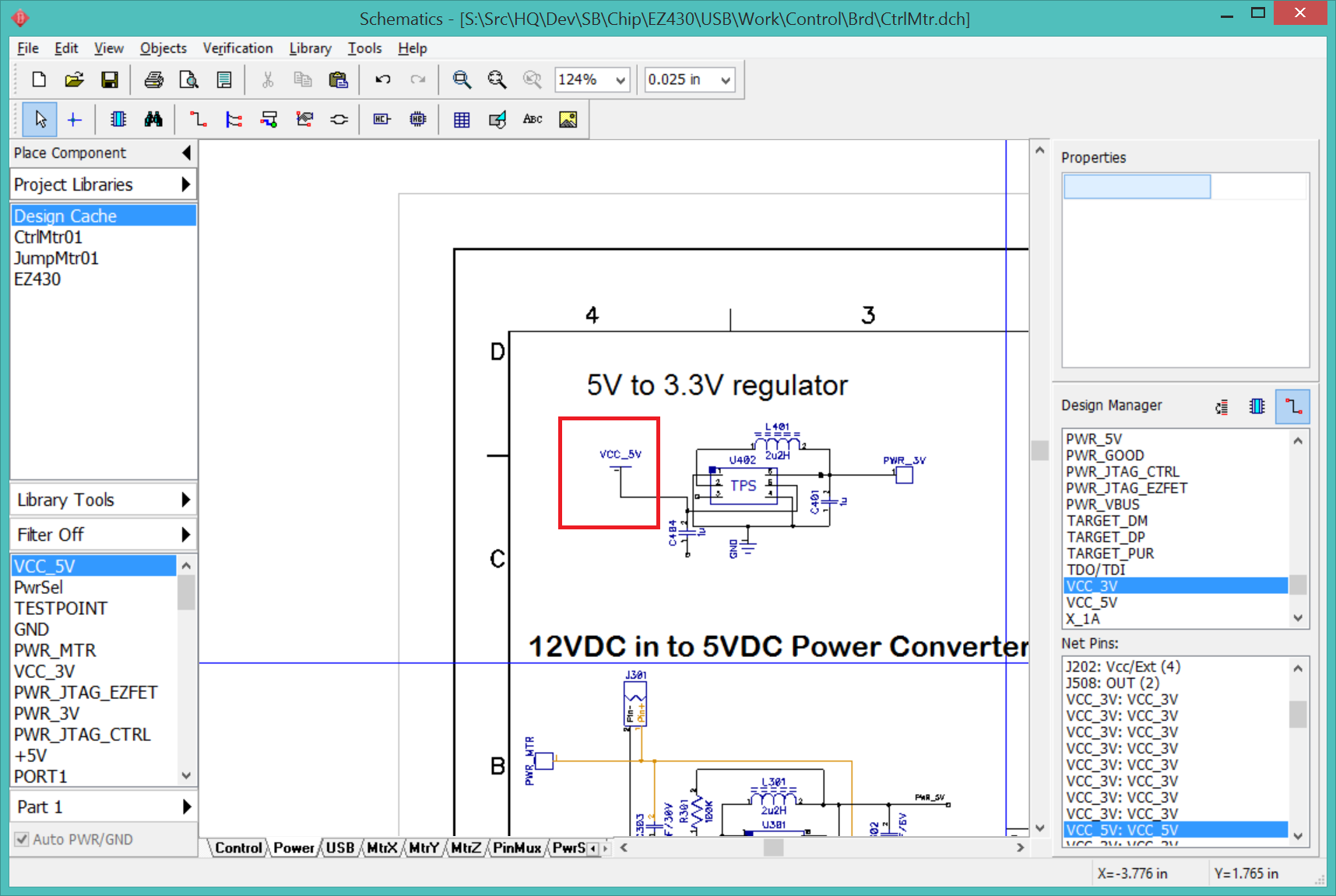
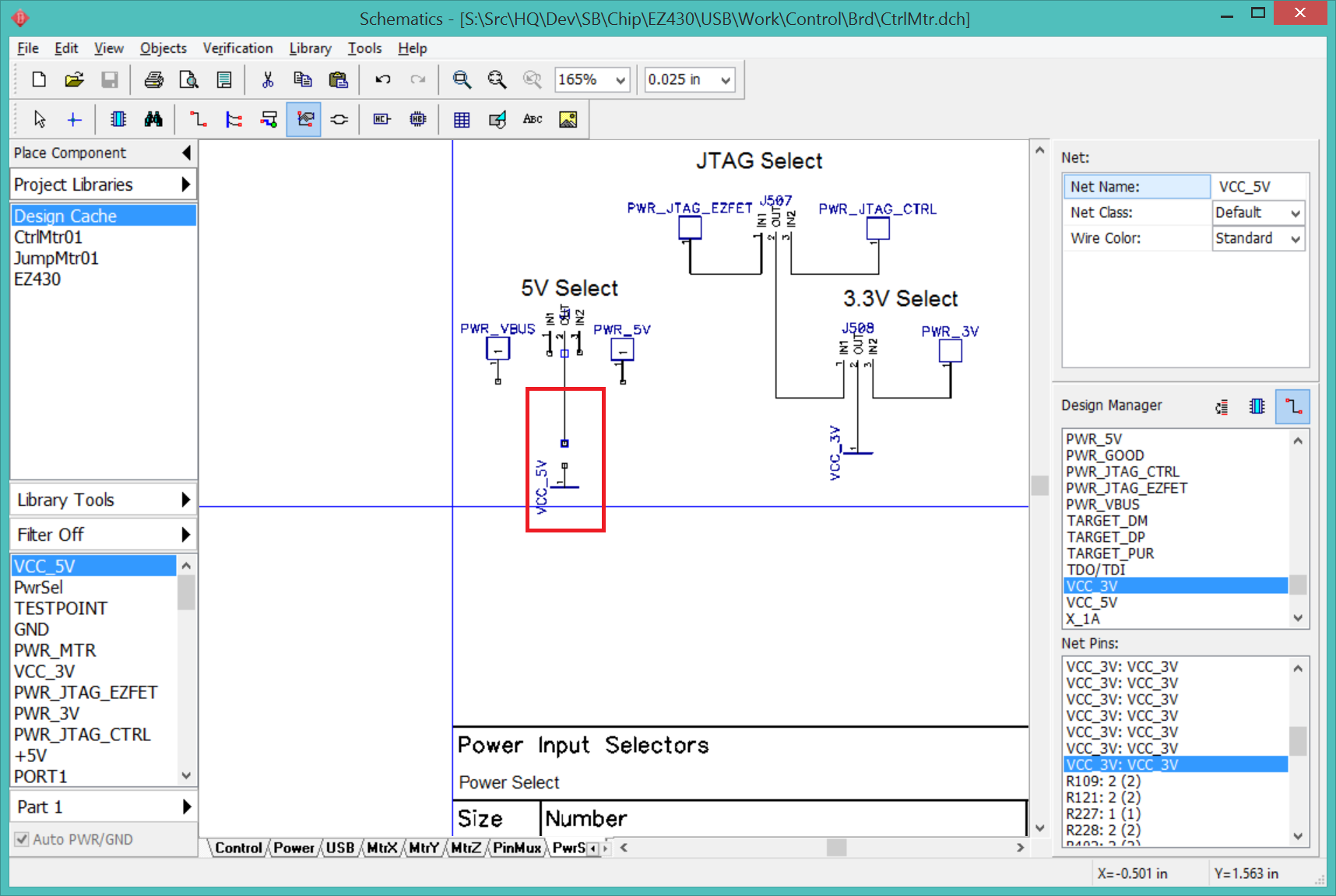
I need to be extremely vigilant and careful when renaming
nets! DipTrace gives very little feedback when renaming nets and I
have freqently renamed, merged, and lost entire nets unexpectedly.
While trying to clean up the VCC_3V and VCC_5V nets I somehow merged
the 5V net into the 3V, resulting in a real mess.
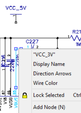
Do not rename a wire by changing the net name from the context
menu. Instead, delete the wire first, verify that the pin has been
disconnected from the net, then recreate the connection to the pin.
The connection can be a wire or a "wireless" connection to a net.
For example, when I select the VCC_3V net in the design manager, I
should not see any instances of a VCC_5V pin. This is where
creating my own VCC_5V net port and setting the pin name has paid off,
otherwise all of the components would be named "PORT1" and the pins
would be named "1". Because this pin now belongs to the VCC_3V net,
any time I try to connect a VCC_5V port it instantly joins the VCC_3V
net. This confused the hell out of my for about 30 minutes. The only
solution I could find was to first delete all the VCC_5V net ports,
then rebuild the VCC_5V net.
After purging all the instances of VCC_5V from the VCC_3V net, I
tried connecting the VCC_5V net port again. This time it finally
worked.

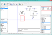
Now I need to go back and reconstruct the VCC_5V connections I just
deleted. This time, checking which net is actually used each time.
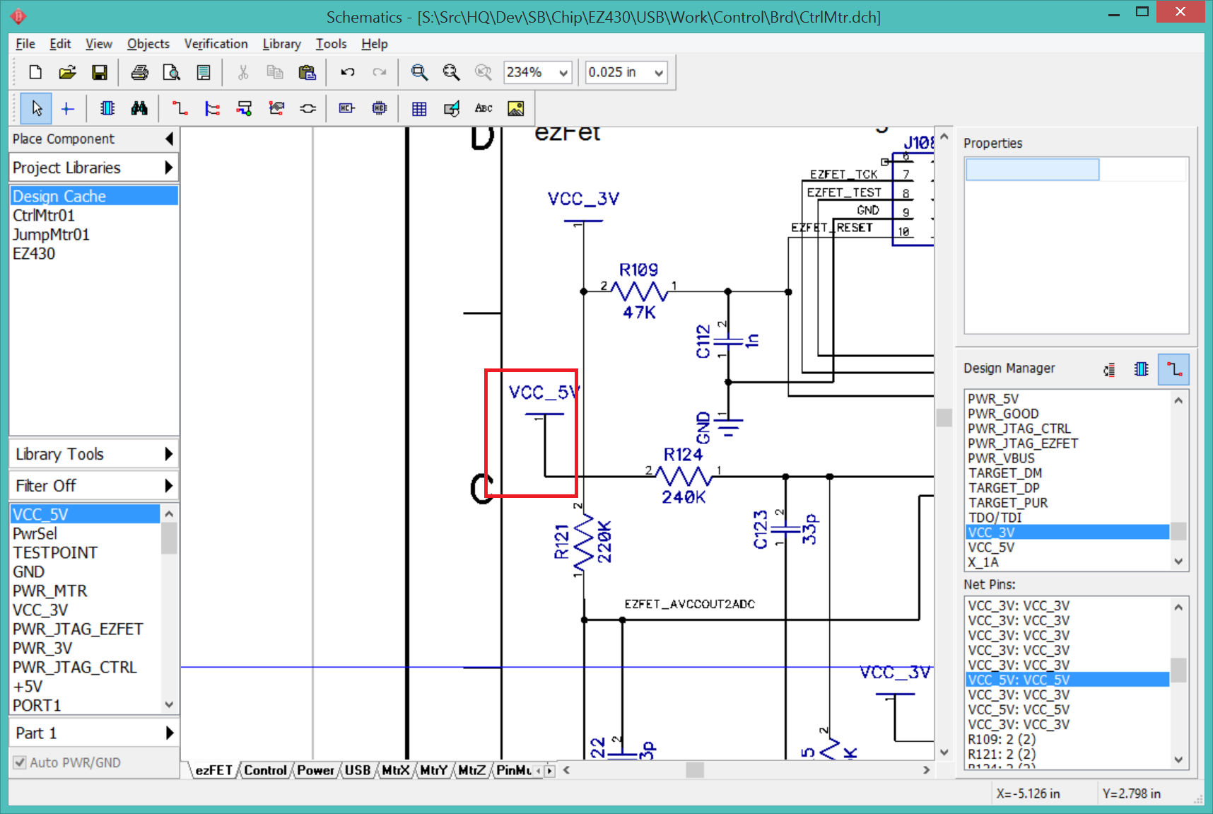
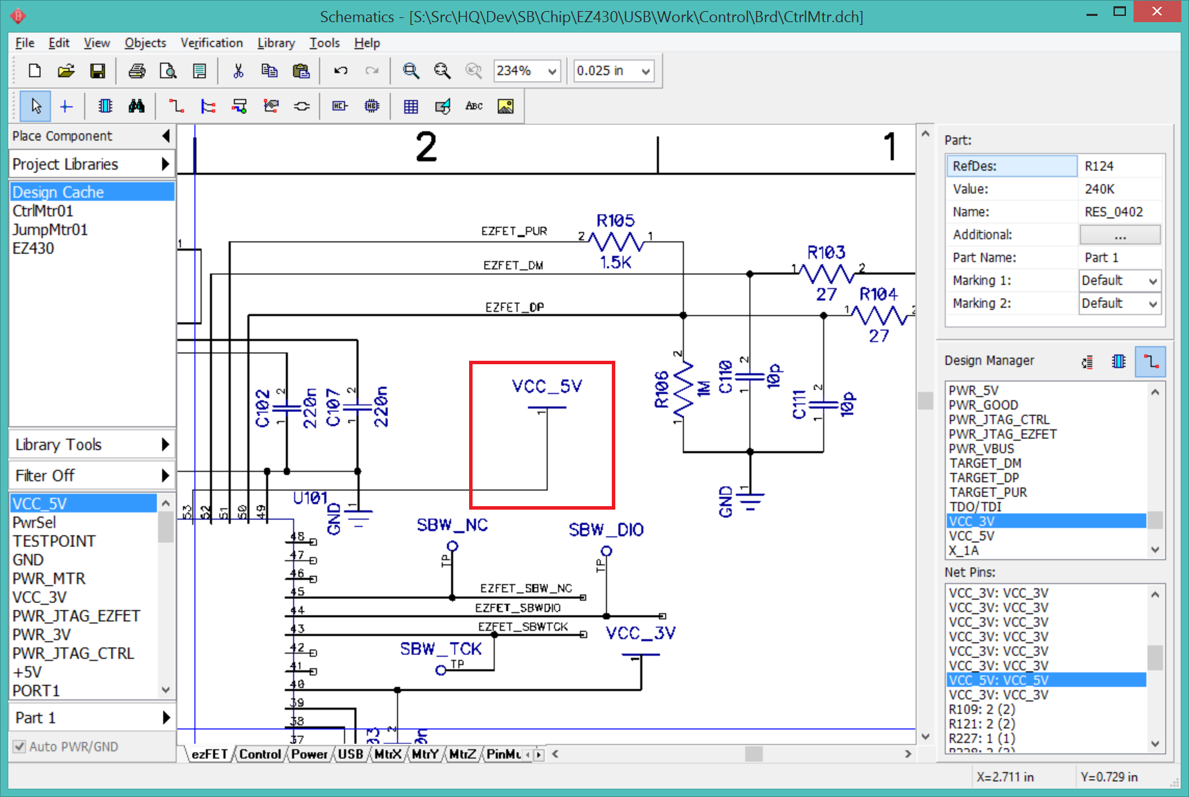
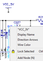
This problem occurs when I notice that a net is wrong and I just
rename it to the correct net. Big trouble if I forget to check
"related wires only" OR if the wire is connectect to an off-sheet
component OR if the wire is connected to a net port. It is safer to
fully deconstruct the wire and rebuild it. In this example, the net
between pin65 and C227 is erroneously set to VCC_3V when it should be
VCC_5V. I can just right-click the wire and rename it to "VCC_3V" with
"related wires only". This usually works as expected, but I need to be
vigilantly watching the net in the design manager. I am finally able
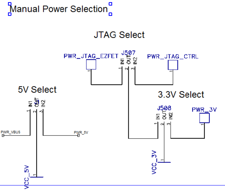
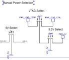
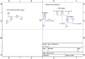
to wire up the power selectors correctly.
I have spent all day fixing schematic problems that were exposed
during the first pass at the layout. It is time for a break, then I
will review the schematic again before attempting another layout.
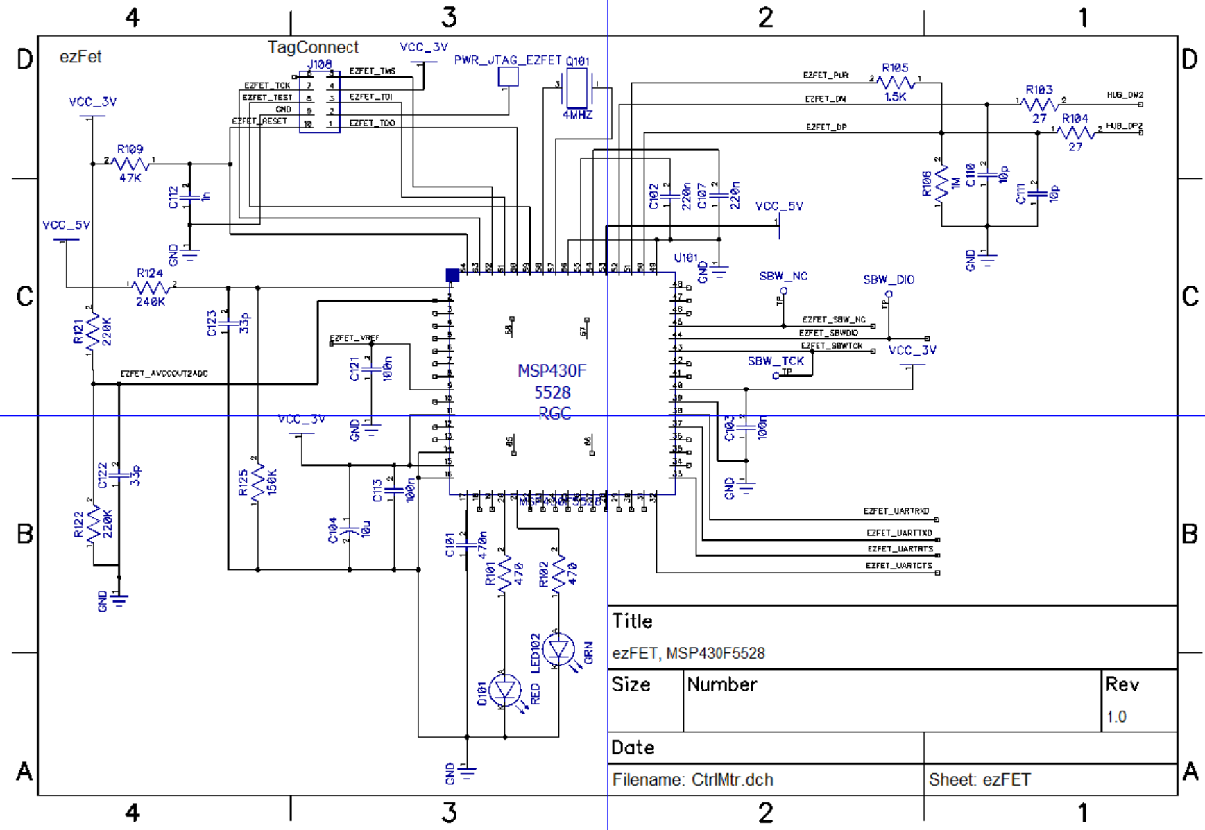
Hopefully I will be able to reuse the existing board. Most of the work
was around the A3967's, and not much changed around those devices.


WebV7 (C)2018 nlited | Rendered by tikope in 127.847ms | 216.73.216.220