April 16 2016
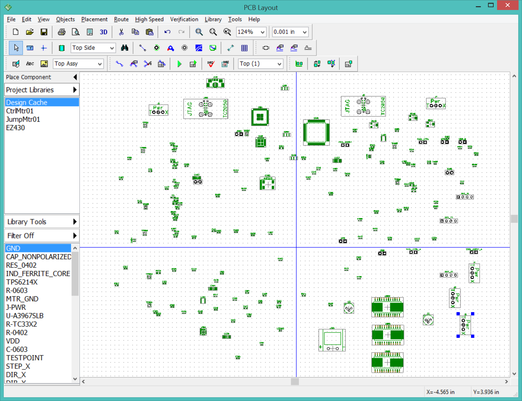
Layout has officially begun. I replaced the reset switches with simple header posts, which finished the first draft of the component library for the project and allowed the schematic to export to Layout. Here are all the pieces to the jigsaw puzzle, now I just need to connect the wires.
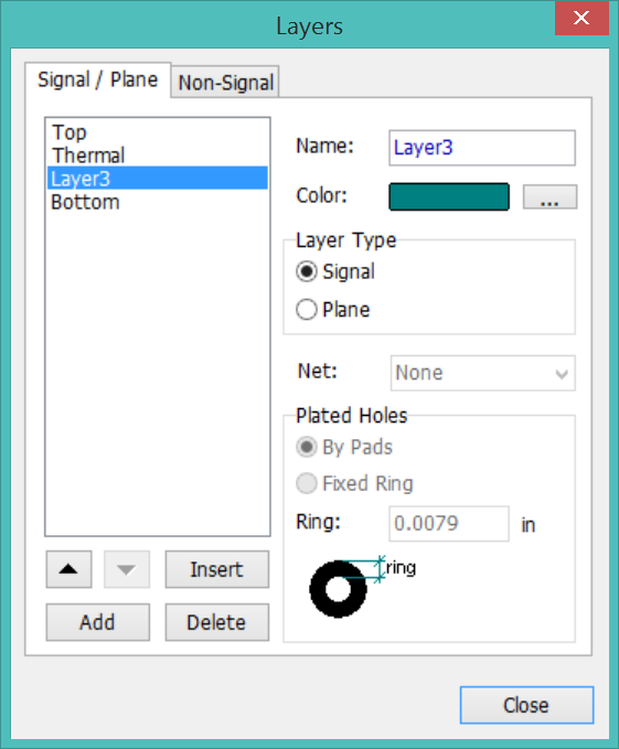
I already know this board will have 4 layers: Top, Thermal, Layer3,
and Bottom. The Thermal layer will also be the ground plane,
consisting of a big copper pour that will be connected to the heat
sink. There can be some signal traces in the thermal layer but as few
as possible and marking it as a plane prevents the auto router from
using it, but does not prevent me from placing traces there manually.
Layer3 will be a signal layer. All vias should be through-hole (no
buried or blind vias) to minimize cost.
Route > Layer Setup...
SparkFun provides some generic guidelines on the design rules to make third-party manufacturing easy. They recommend using part no smaller than 0603, which surprises me. I have no problem with 0402, and any IC in a 0.3mm or even 0.5mm pitch VQFN will require the same placement and stencil tolerances as an 0402 resistor.
HINT: Avoid running parallel traces over each other on multiple planes, this creates an impenetratable wall. Whenever possible, use one plane for North/South and another plane for East/West. Keep traces on the top layer short, this will be the most convoluted layer due to the components.
The hardest parts to route are the ones with the most pins, these cause a lot of congestion. So they are the ones to sort out first. I start with the MSP430F5529. It doesn't need direct access to anything on the edge of the hub (ie power terminals, usb connectors, etc) so I can move it to the center. The JTAG interface can go anywhere nearby, the cable connects from above.
I need my ratlines to know which pins need to be connected. First
renew the layout by RefDes
File > Renew Layout from schematic... > By RefDes > CltrMtr.dch > Use
PCB layout settings. This creates the ratlines. They are named "rat
lines" because it initially looks like a rat's nest.
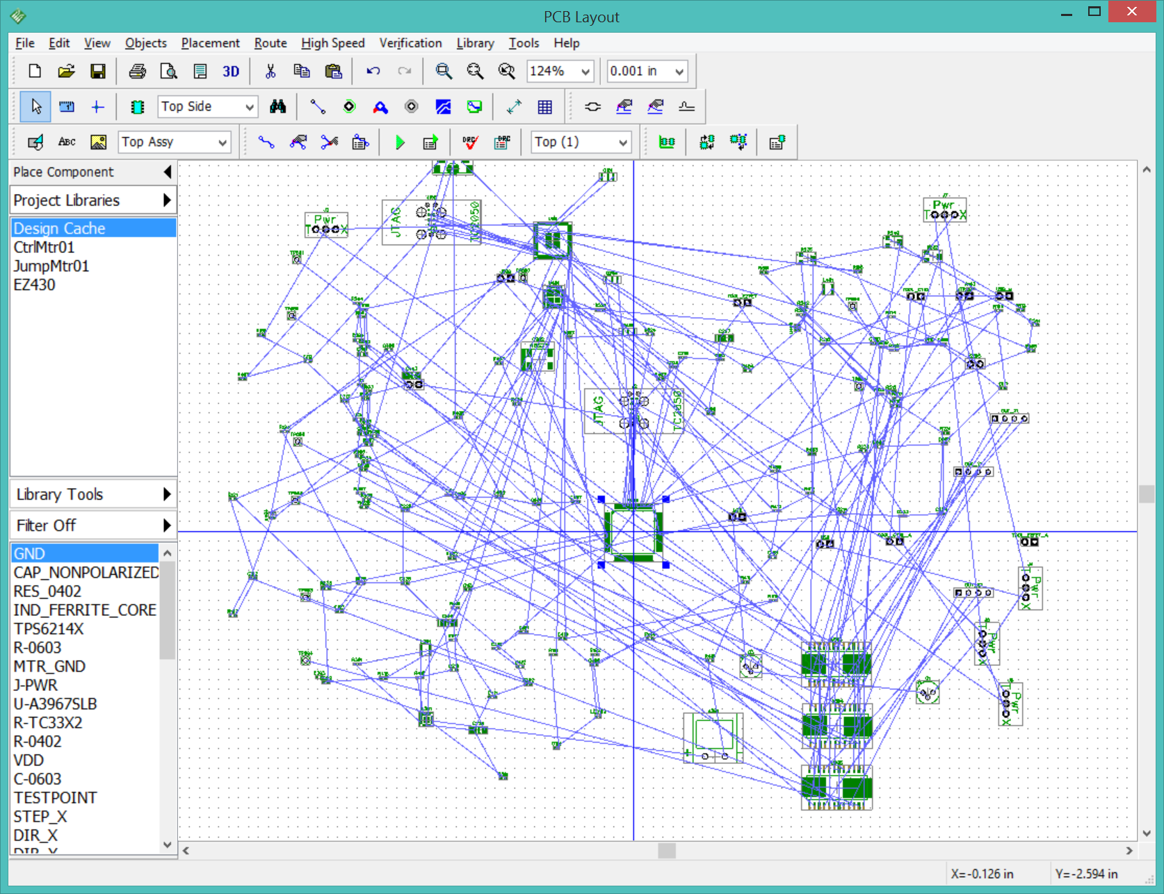
I let DipTrace create the first rough draft. My experience with DipTrace v2 is that the auto placement and route was not very good. Let's see if v3 has improved... Run auto placement first, then auto route. This will take a while, there is plenty of time for a coffee break. Auto placement finishes after about five minutes.
The auto placement looks fairly good. It isolated the motor drivers, which is a good thing. The board is 5x5" with lots of empty space, so I expect the final board might be around 3x4".
I save the layout, and just as a preview I run the auto router. It finishes after about five minutes. There are only 2 unrouteable ratlines.
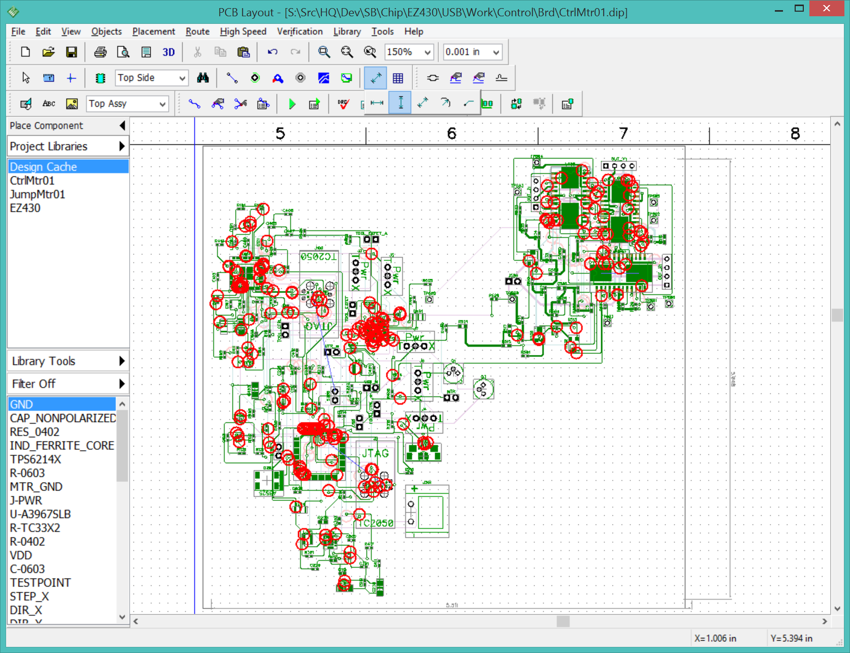
That is good for a preview. It gives me an idea of the size of the board and where the complicated areas to watch. I undo the auto route since I want to rearrange the components. I know that the main motor power lines need to run in a line under the A3967's so they need to be rearranged into a line. I want the motor terminals to be close to the A3967's.
I forgot to remove my "automatic power selection" circuit before exporting. DipTrace doesn't give me an option for "do not populate" so I need to simply delete it from the schematic and renew the layout. Easy, and it removed some trouble spots.
Don't spend much time thinking about the perfect layout at this point. I want to make as many connections as possible, as quickly as possible, and identify the problem areas early.
Look for any components with only a single ratline, this is probably a broken connection. For example, R231 is supposed to be connected to HUB_DM but this net isn't connected to anything. Apparently the net names were messed up when I copied them. There were two problems, TARGET_PUR was connected to TARGET_DM when it should have been connected to TARGET_DP. HUB_DM and HUB_DP should have been HUB_DM1 and HUB_DP1. Save and renew.
I will be renewing the layout fairly often as I correct problems in the schematic and components. To avoid having DipTrace constantly complaining about different net widths, I take the time to update the net classes in schematic to match layout.
| Class | Width | Clearance |
|---|---|---|
| Default | 0.008 | 0.005 |
| PWR_DATA | 0.015 | 0.005 |
| PWR_MTR | 0.025 | 0.010 |
| HEAT | 0.008 | 0.005 |
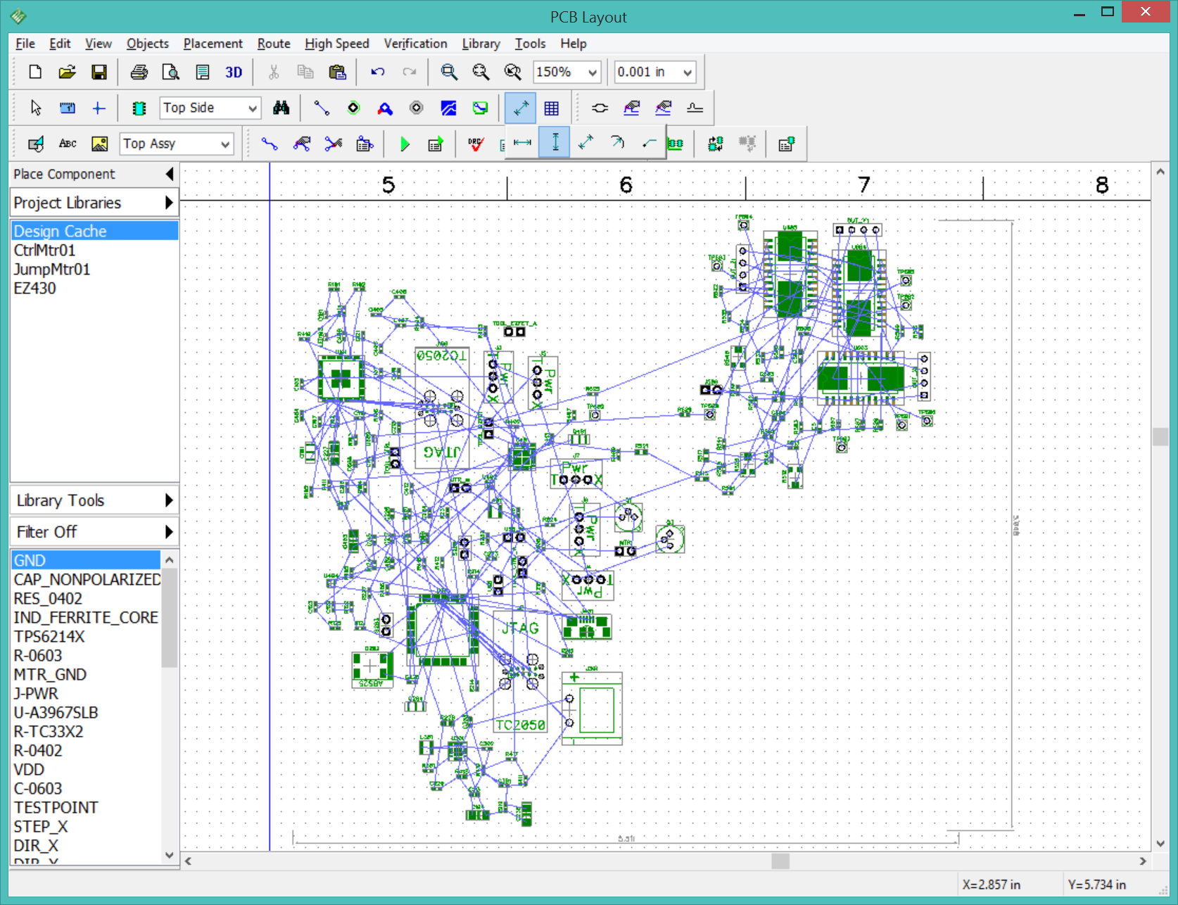
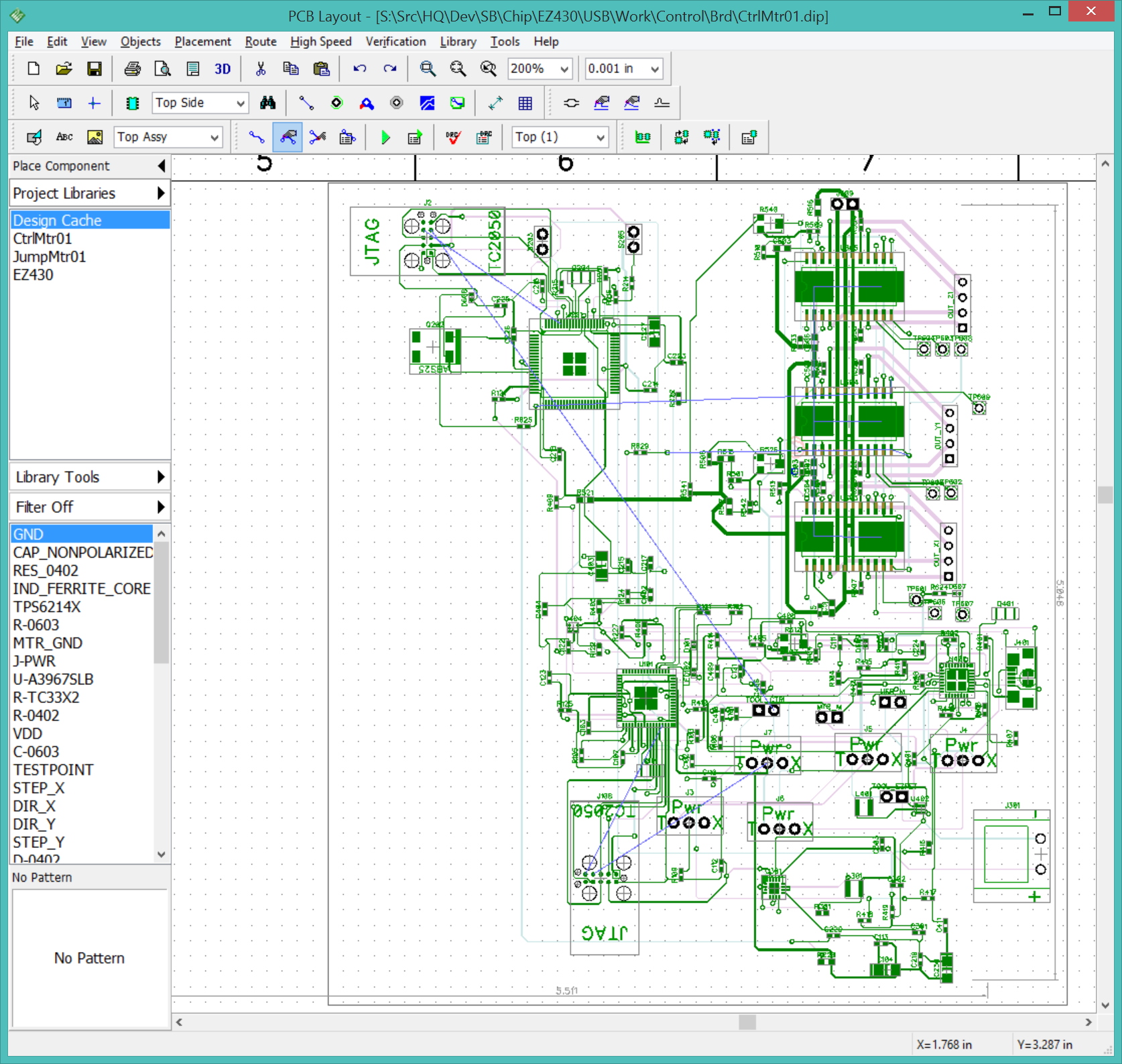
10:46> I run the auto router again with the revised layout. It completes in less than a minute, a sign that the new placement is much better.
11:12> The net classes for PWR_DATA and PWR_MTR needed to be updated. It would be nice if I could specify a net class on the component pins. Instead, I need to remember to assign the net class after placing the wire on the schematic. The net classes need to be updated in the schematic so they will be preserved when I renew the layout.
There is a problem with GND. There are actually two ground nets, one for the motors and the other for everything else. They should be isolated by the 0-ohm resistors. Currently, they are comingled. UPDATE: The ground and power nets are isolated into PWR_MTR, PWR_GND, and GND. The power nets in the PwrSel sheet need to be sorted out.
The JumpMtr2 layout should be used as a reference for laying out the A3967's and the motor power lines and terminals. It can't be copied straight in, but it can be used as a guide.
13:00> I started working on the motor controllers first, it seemed to be the easiest target. It is mostly routed, not optimally, but enough to diminish the clutter enough to see what needs to be done. One of the challenges when starting to layout is that the ratlines can be misleading. The GND touches a huge number of components, but the ratline only points to the nearest ground pin. Frequently, the nearest neighbor is not the best place to connect.
April 24 2016
I am finally pulling the functional blocks together. This layout has the motor power terminal block, motor drivers, power converter, voltage regulator, power selectors, and 5529 pulled together into a 3x3.25" area. The control signals to the motor drivers and the power to the 5529 are all wired up.
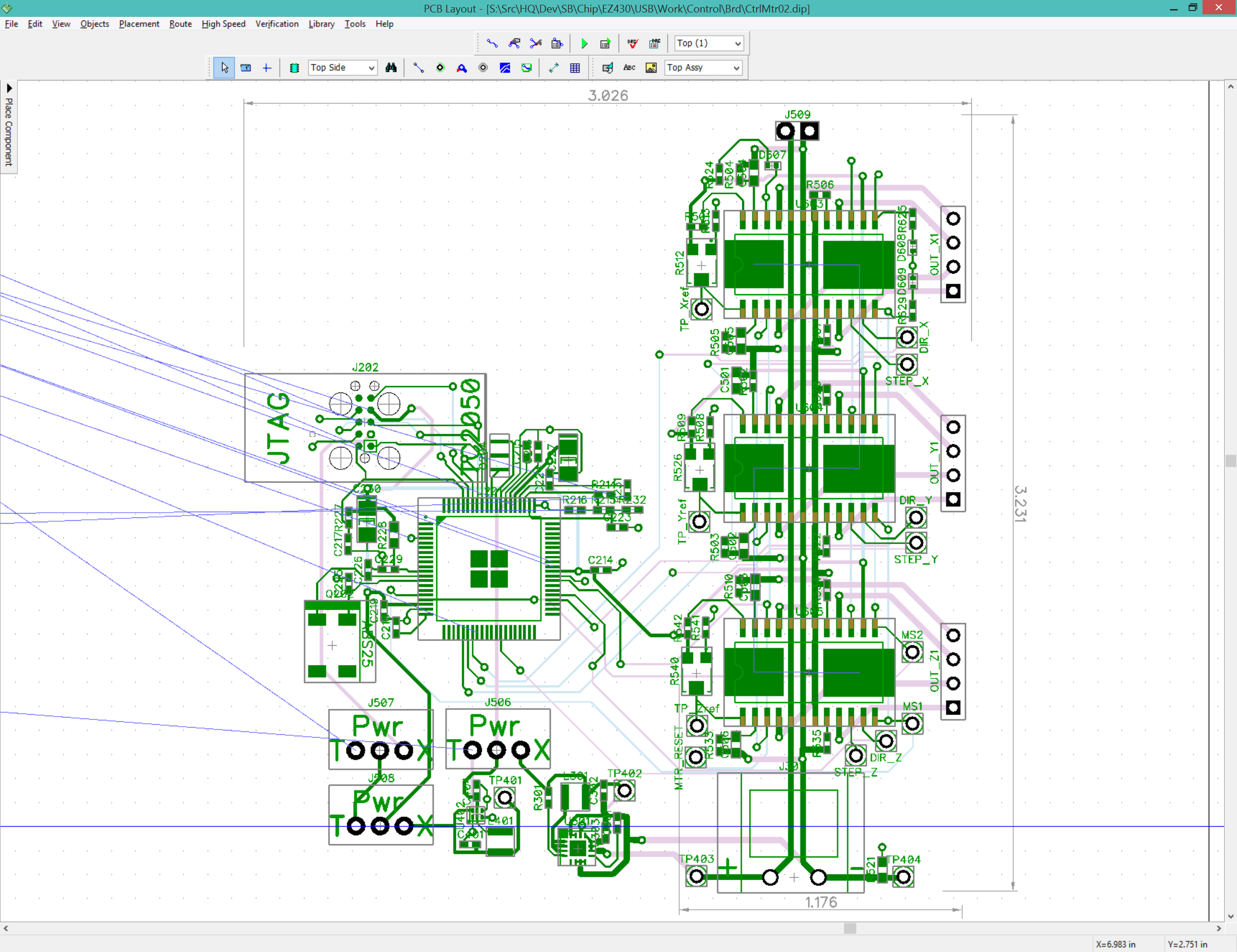
I pulled in the MSP430F5528 and connected it to the 5529.
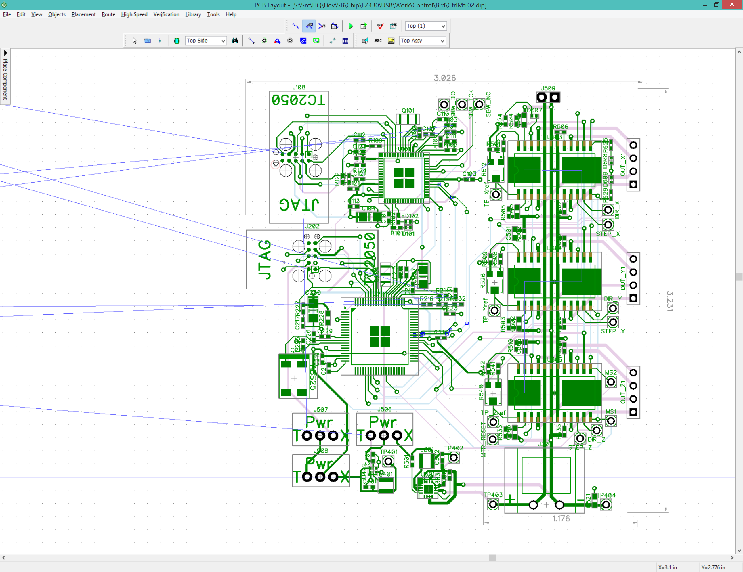
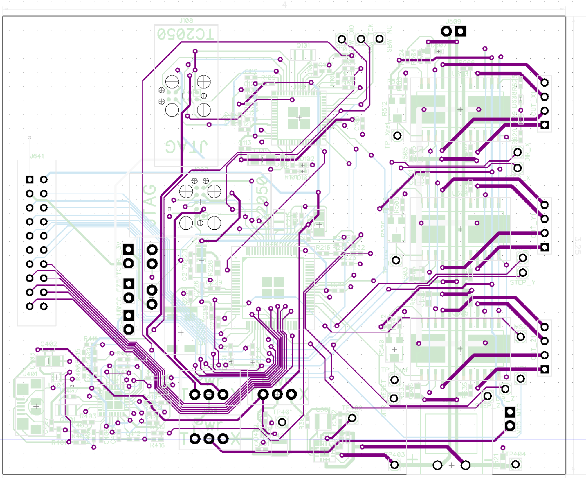
April 24 2016 11:00pm> CtrlMtr02 is now fully routed! Board area is 4x3.25" with space reserved for an expansion header.
I left HEAT as a distinct net, I did not merge it into GND. I am sure this will make little difference to the thermal dissipation. DipTrace does not merge nets well and I didn't want to add a BRIDGE2 test point for this.
April 25 2016
I am reviewing and polishing the layout. I added two general purpose leds, the expansion header, and jumpers to isolate the 3.3V supply to the 5529, ezFET, hub, and motor drivers. I wanted to isolate the VCC_3V for two reasons, first to de-power the other components while I am debugging the 5528 or 5529 using the JTAG probe, and second to de-power the ezFET and motor drivers if I wanted to use the 5528 as a generic experimenter's board.
The mounting hole corners are (2.87in,2.87in) and (6.62in,-0.13in), making the mounting dimensions 3.75" x 3". It is important to write this down since I will lose the mounting holes and fiducials every time I renew the layout from the schematic.
April 26 2016
I realized I had not connected the ESTOP or /SLEEP signals to the 5529, both of which need an indicator led. ESTOP also needs to connect to the expansion header (pin 20).
Layout is complete, it is time to move on to procuring parts. I have added some parts since I last reviewed the BOM, so the first step will be updating it.
May 3 2016
The parts have arrived and I am beginning the paper board build. The final touches to the board include placing the mounting holes and fiducials. These virtual components will need to be added to the layout again whenever the layout is renewed from the schematic.
| RefDes | Item | X | Y |
|---|---|---|---|
| A1 | Hole | 2.87in | 2.87in |
| A2 | Hole | 6.62in | 2.87in |
| A3 | Hole | 6.62in | -0.13in |
| A4 | Hole | 2.87in | -0.13in |
| F1 | Fiducial | 3.00in | 2.70in |
| F2 | Fiducial | 6.50in | 2.70in |
| F3 | Fiducial | 3.40in | 1.00in |