September 11 2014
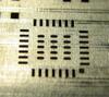
I spent some time thinking about heat dissipation. BlinkMtr01 proved that the A3967SLB controller kicks off a fair amount of heat. BlinkMtr01 had no heat sinks other than the solder masked board surface and the pads, and it would quickly heat to over 200F under only a light load. I added a small copper pour to the top layer of BlinkMtr02 to serve as a heat sink, and this was a big improvement.
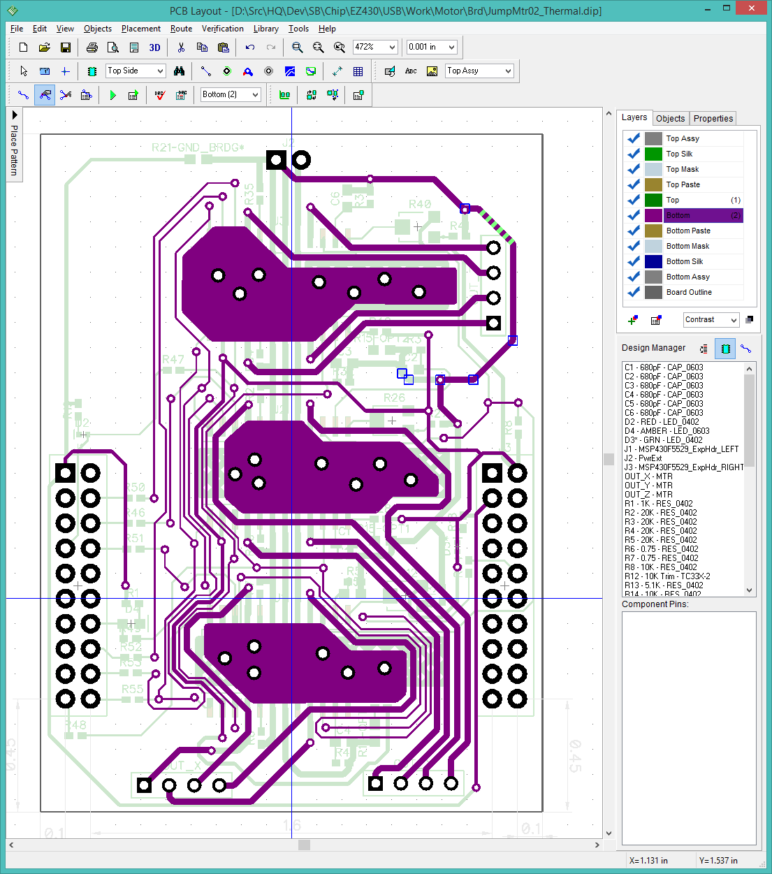
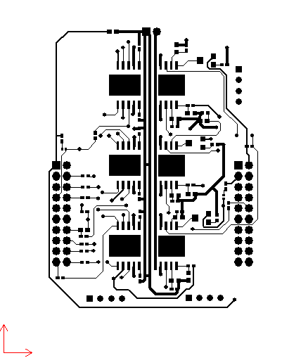
JumpMtr has three A3967SLB controllers, which means three times the heat. I increased the heat sink area dramatically by placing a second, even larger, copper pour on the bottom layer. I had to shove some traces around to make room.
The trick was figuring out how to physically connect the copper pour on the top layer to the copper pour on the bottom layer. I tried creating static vias, but DipTrace would isolate them. Eventually, I realized that DipTrace's job was to ensure connectivity to nets, and conversely make sure no nets touched any other nets. So I added the copper pours to the MTR_GND net, then placed through-hole pads to drill the connection from the top to the bottom layer.
To do this:
This looks like it should work. Improvements might include:
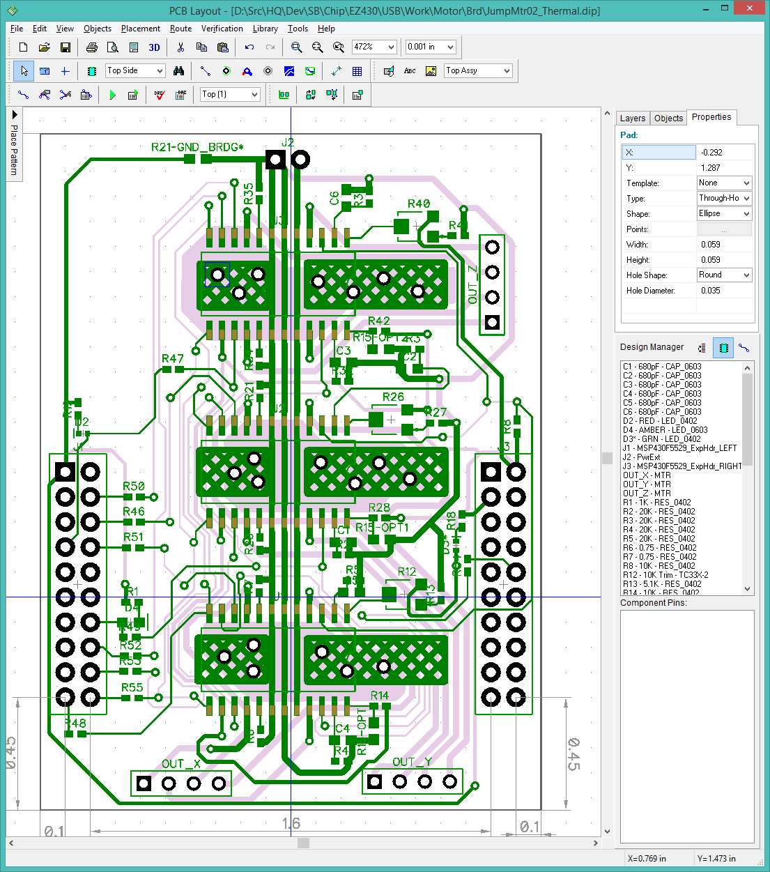
I noticed a problem with the layout above: There is still solder mask over the top copper pour, which would block the heat flow into the copper. I vaguely remember dealing with this in the BlinkMtr02 project and solving it using a separate overlaying shape in the top mask layer. This solution means managing the solder mask shape, heat sinks, and connections independently in the layout. This is a nuisance, especially when there are multiple copies of the component.
A better solution would be to make the heat sink integral to the component. So I reopened the component library...
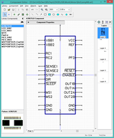
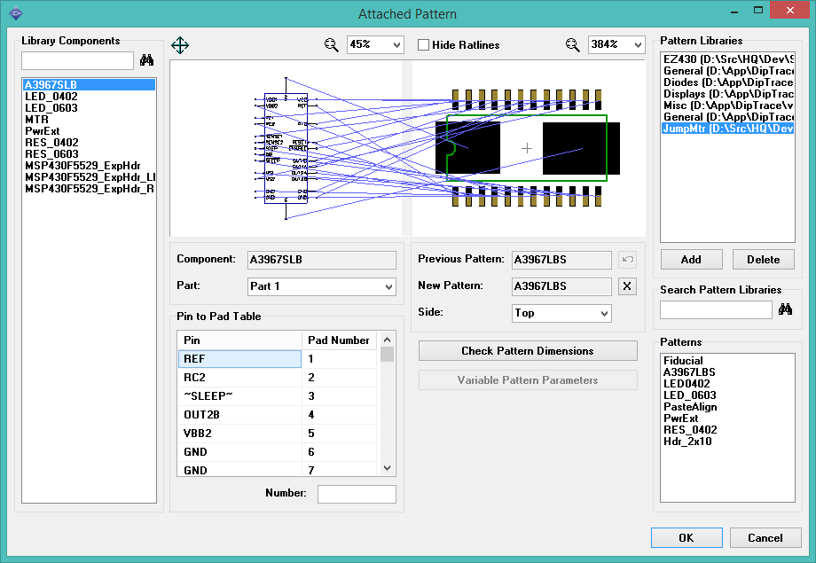
I opened the existing A3967SLB component and added two new pins, pin 25 and 26, both named "HEAT". I need to create a dedicated heat sink net.
I launched the Pattern editor, opened the existing A3967SLB pattern, and added two new surface pads, 25 and 26. I then played around with the pad dimensions until they filled as much of the underside of the component as reasonable. Since these are surface pads, there is no solder mask. I want to disable the solder paste also, so I right-click each pad, click "Mark / Paste Settings..." and disable top and bottom paste mask. Save the pattern library.
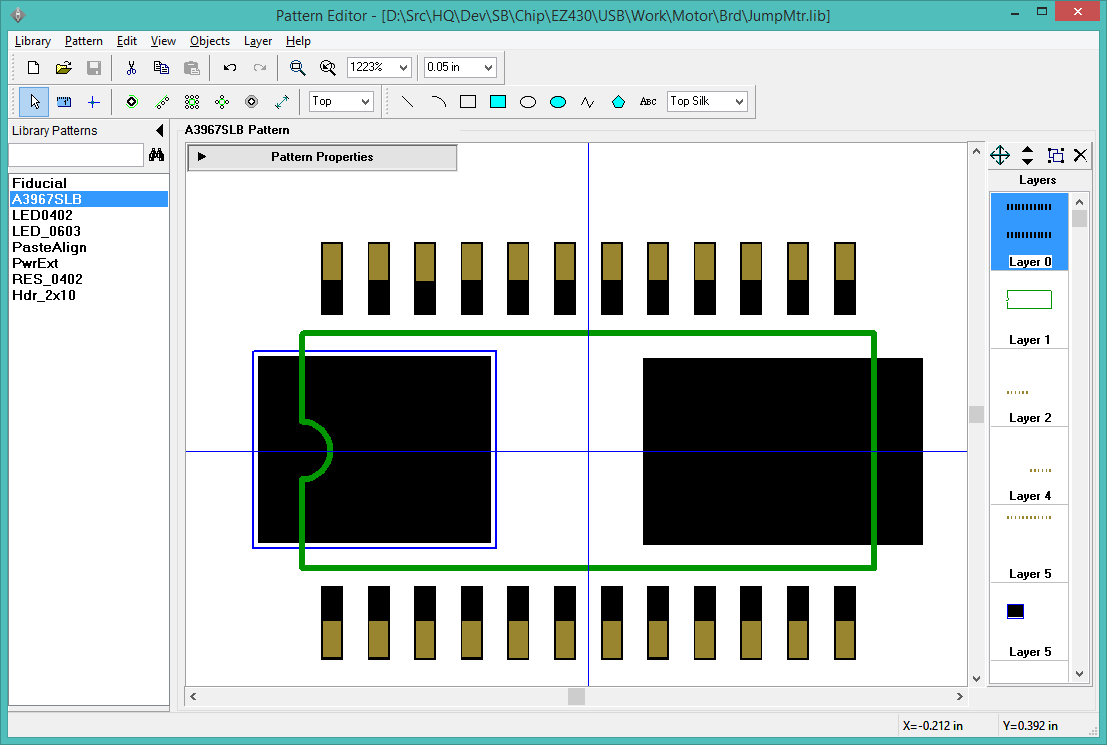
Good thermal pads
UPDATE 20141023: I found a blog post at Screaming Circuits (PCB design partner for Sunstone) that talks about the proper size of ground/thermal pads to prevent the IC from floating during reflow. I should revise my pattern for the A3967 to include several small pads in the solder paste layer. This will provide better structural strength and thermal flow into the copper pours. I have also been told that the solder mask does not impede thermal flow much. So rather than a large open pad in the solder mask with no solder paste, it is better to have several small regular pads (solder mask + paste) that connect to the copper pour using a thermal net.
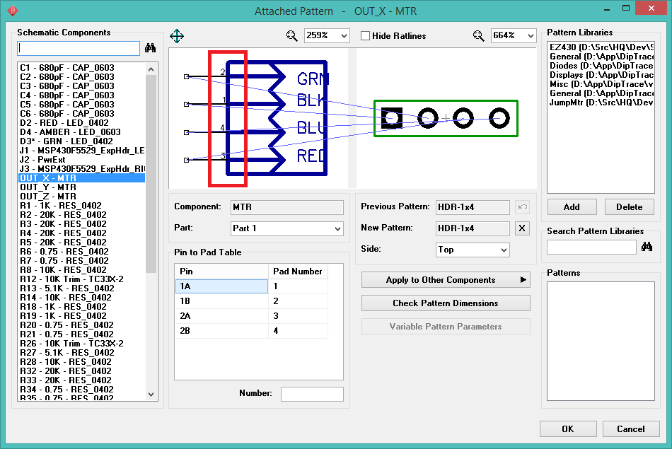
I need to go back to the component editor and update the new attached pattern. Open the component, click Component > Attached Pattern... Then click JumpMtr under Pattern Libraries to reload the pattern. Verify that the new heat sinks are present and that pins 25 and 26 are connected properly. Save the component library.
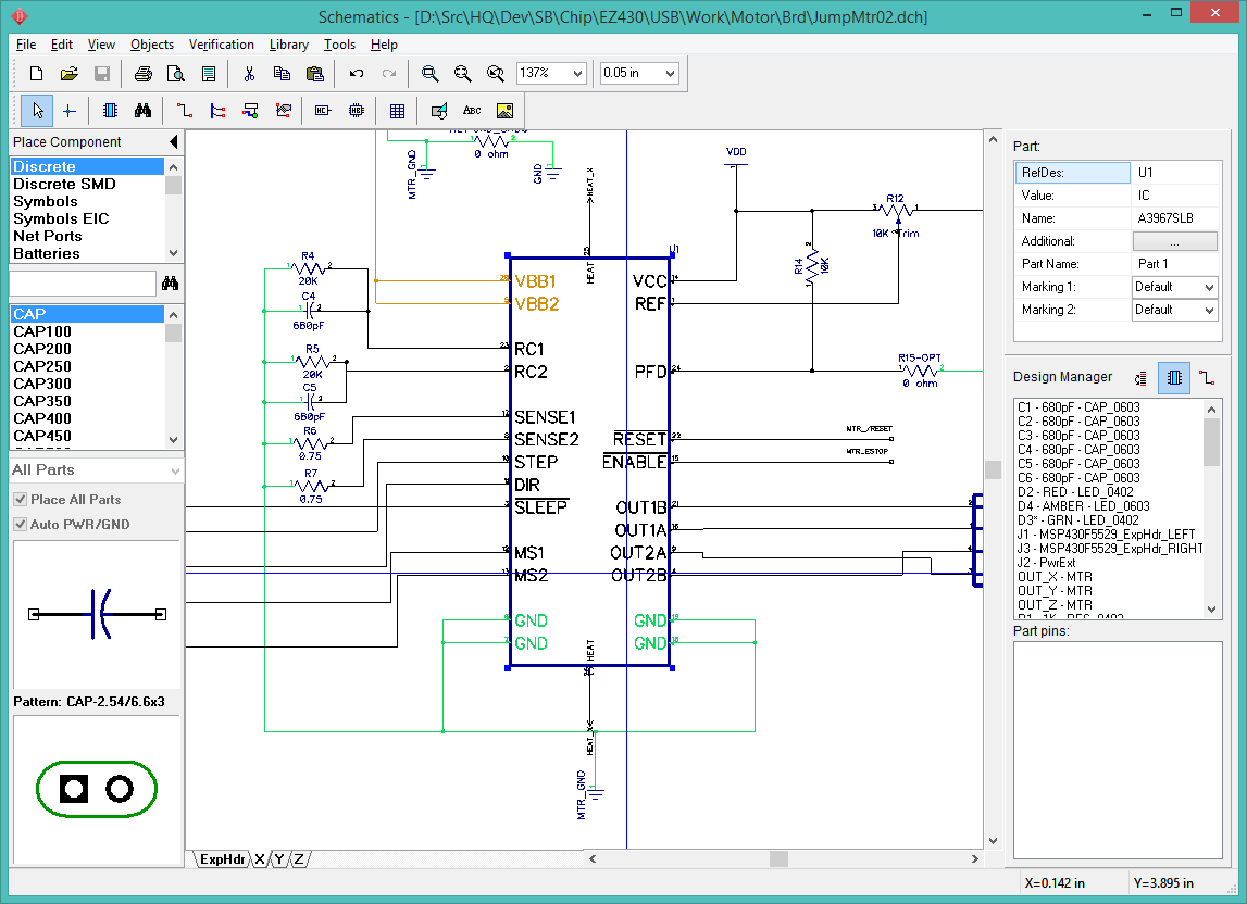
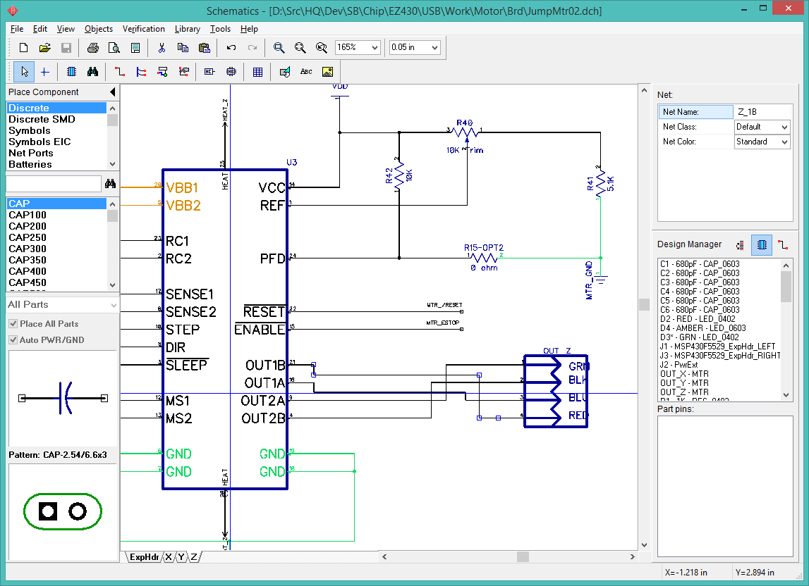
I need to update the schematic with the modified component. Launch Schematic Capture, open JumpMtr02_Thermal. Right-click on one of the A3967SLB components and click "Replace Part...", "Updating from Library" does not seem to work as expected. Select the JumpMtr01 library then the A3967SLB component and verify that the new HEAT pins are present. Select Apply to Similar named components and click OK. The schematic should now have two HEAT pins protruding from the top and bottom of the A3967SLB components.
I am not using a dedicated thermal/ground plane, I am just creating copper pours on the bottom layer. These pours need to co-exist with the bottom signal traces, so I will need isolated pours for each of the three heat sinks. So I create a new net for each of the pair of HEAT pins on each driver: HEAT_X, HEAT_Y, HEAT_Z.
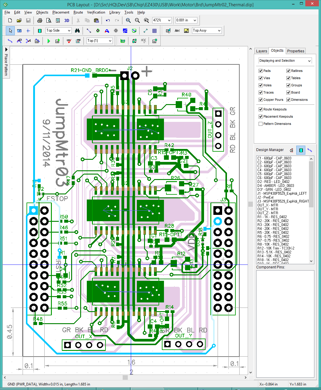
I need to update the layout with the new components and nets. I launch PCB Layout and open JumpMtr02_Thermal. The first thing is to remove the existing top layer heat sinks, they will be replaced by the HEAT pads. Leave the bottom pours in place. Then right-click a A3967SLB, click "Update from library... > Similar named components". This should replace the existing pattern with a new pattern that has two large pads under the body. Hover the mouse over a pad to confirm that it is in the appropriate HEAT_X, HEAT_Y, or HEAT_Z net.
Go to the bottom layer, and for each of the three copper pours, right-click Add to Net and move the pour into the appropriate HEAT_X, HEAT_Y, or HEAT_Z net.
Now I need to connect the top pads to the bottom pours. I do this put routing a trace from the first top pad (hit 1) down to the bottom pour (hit 2), to under the center of the other pad (indicated by the other end of the ratline), and finally up to the other top pad (hit 1), and done (hit Enter). I need to do this to satisfy the net connectivity check for HEAT_Z. I should be able to simply drop static vias, but this leaves the ratline on the screen even though the connectivity checks out OK. Basic connectivity is now done. I scatter a few more static vias in the HEAT_Z net to improve thermal flow.
Andrea from Bay Area Circuit replied:
I would setup the pours as solid and enable the thermal connections for the components.
We can drill at 6 mils and the hole may or may not plate shut. However are web orders do require a 10 mil min drill size. Conductive filling is also another process that adds additional cost. I would need to provide you with a custom quote if you would like to go this route.
The best thing to do is to place several vias evenly spaced around the solid pour. The vias don't need to be thermal type. Thermal connections are mainly for component leads, they ensure that the solder will flow correctly.
Removing the Soldermask will have a negligible effect. If there area is safe from shorting you can remove it if you want. If heat is that much of a concern you may want to think about adding a heatsink component to the design.
This means I should create a "Thermal" via class with hole size of 0.010" and use that for all my thermal vias. (DipTrace allows creating via classes, but I don't see how to edit or rename them, so my "Thermal" class is named "ViaStyle1".) On further reflection, the 0.010" vias may not be better; the surface area of the via (the perimeter) increases at 3X the diameter, so larger vias have more area. Plus, fewer drill sizes is better. I will keep the thermal vias at the default size.
DipTrace makes dealing with the thermal vias a real pain. They are hard to select because they are within the HEAT pads. They create false ratlines because they connect to different places inside the same components (HEAT pad and HEAT_Z copper pour). There seems to be no reliable way to select multiple vias and add all of them to a net in a single operation. "Add to Net > selected" doesn't seem to work as expected. Tedious, times 3.
It took about an hour or so, this is the result:
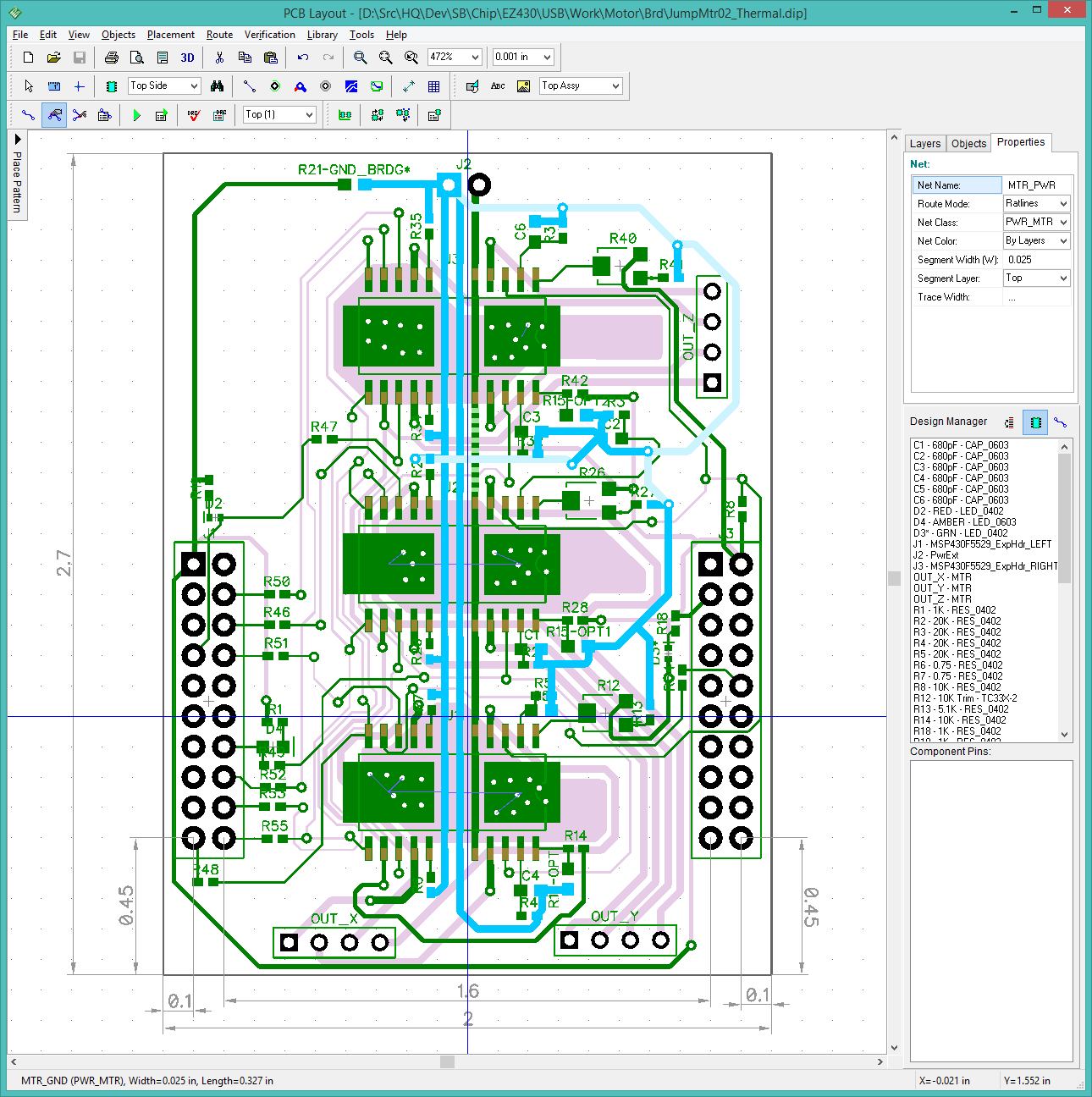
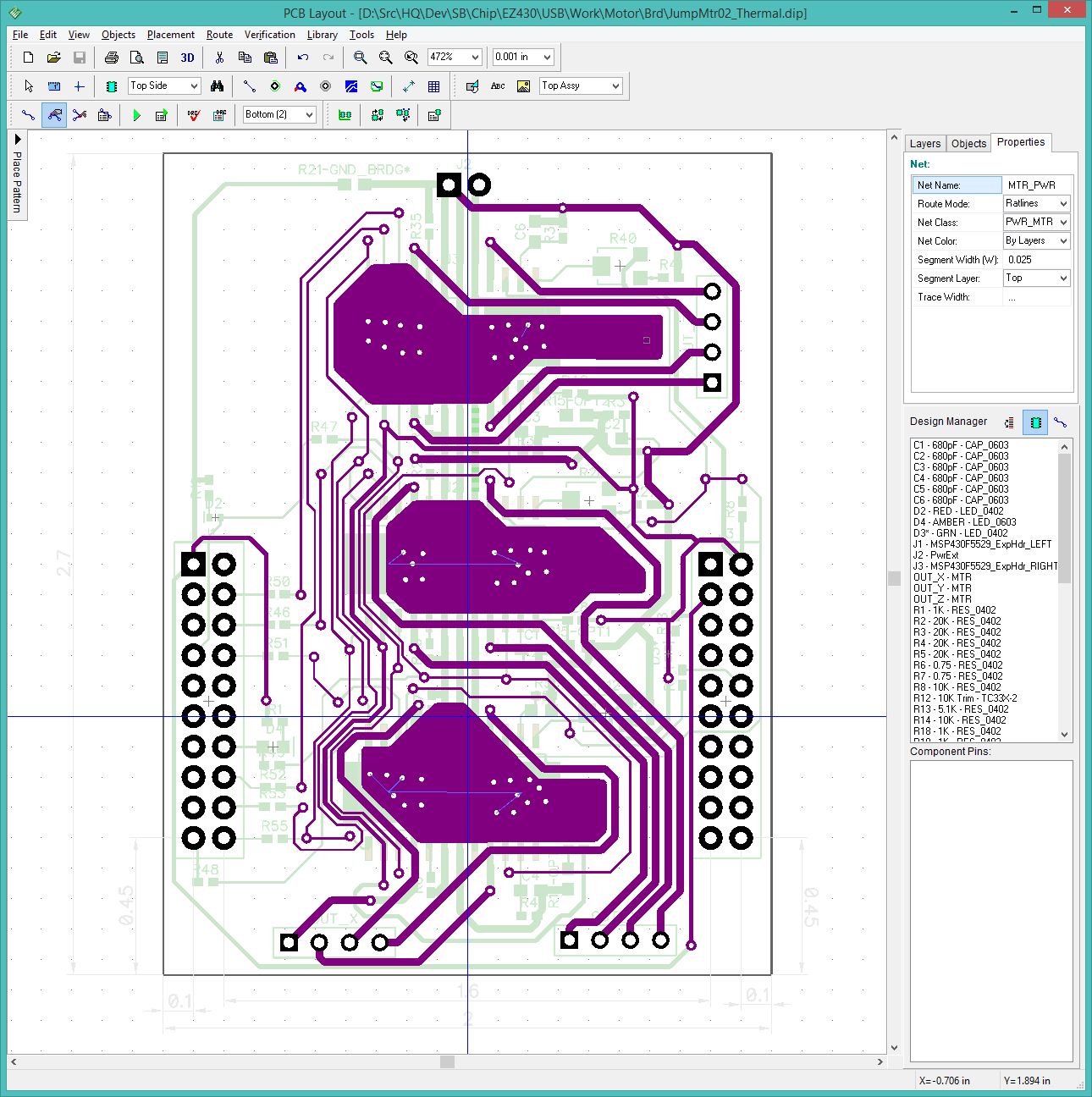
I had to add a redundant trace from MTR_GND to Y.C1 to remove a leftover ratline. The net connectivity checked out OK, but the ratline persisted. I wonder if it has to do with fanout?
There are also leftover ratlines between the thermal vias. I tried to eradicate them without success. Again, the design checks out OK.
Final step is to stare at it for a while, add the fiducials, mounting holes, and printed info.
During my final review I noticed that I had somehow managed to get the motor output pins wrong -- again! I traced it back to the component library, where the pins were in the wrong order. It is amazing how confusing simple connections can be when everyone uses different terminology!
I now believe that BlinkMtr02 worked, but was running the motor
in reverse. Going back to the EZDriver, his output jack used:
1 2 3 4
OUT2A OUT2B OUT1A OUT1B
Looking at the physical wires on the actual motor:
WIRE: GRN BLK BLU RED
COIL: C A D B
STEP: OUT2A OUT2B OUT1A OUT1B
PIN: 1 2 3 4
I swapped the pins in the component library for the motor output connector, replaced the part in the schematic, triple-checked the connections, and reconnected the motor outputs.
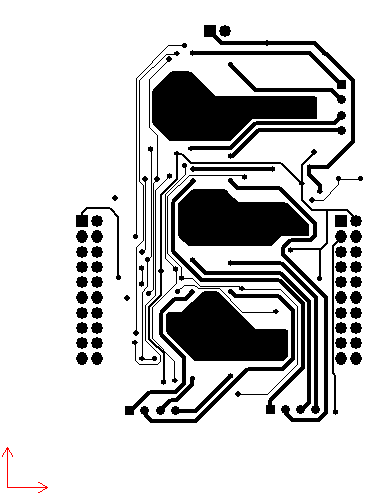
Here is the revised schematic for the motor output connector:
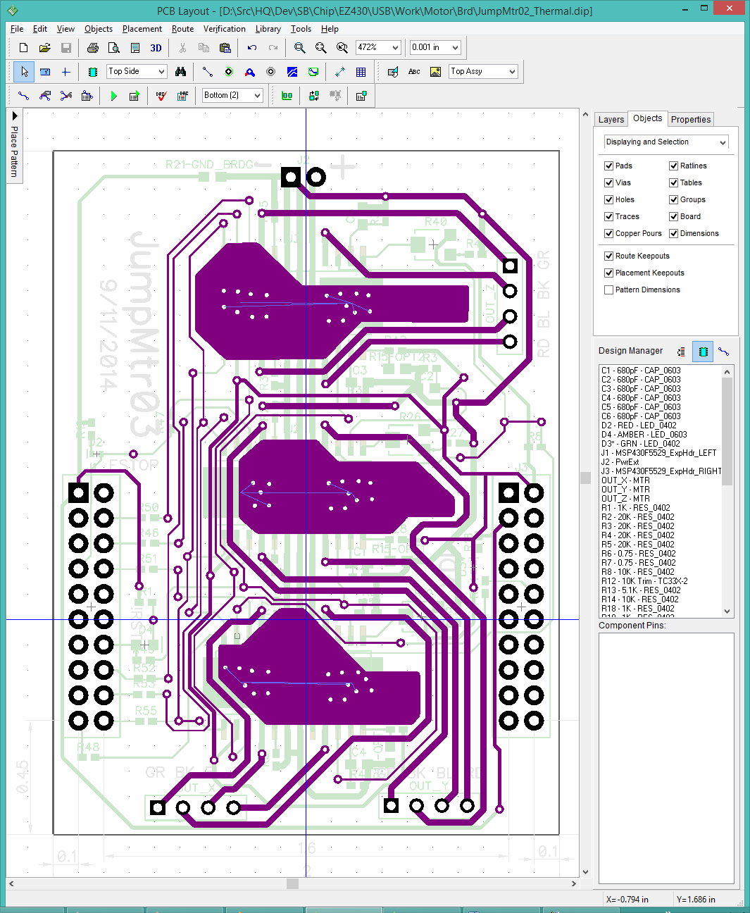
I renewed the layout from the revised schematic, and this is the result. Not too bad...
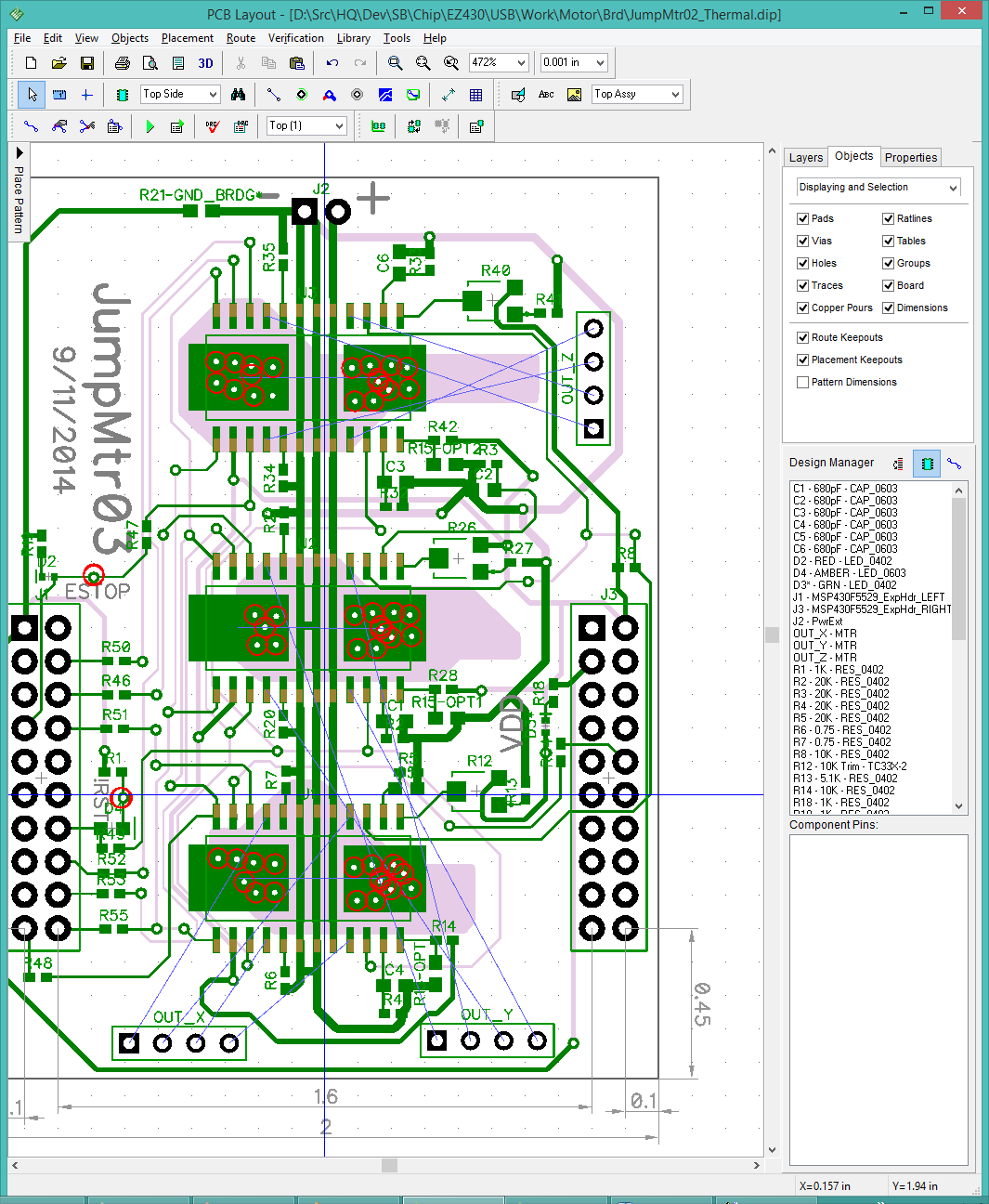
About an hour later, most of which was spent futzing around with the thermal vias...
If this is wrong, I will scream. I have a sick feeling that this particular motor has swapped the red and blue wires. :(
I review the gerbers to make sure everything looks OK, particularly with respect to the heat sinks. In order of TOP MASK, TOP PASTE, TOP COPPER, TOP TRACES and VIAS, and BOTTOM COPPER.
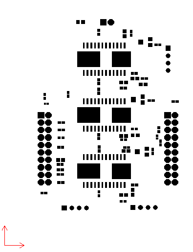
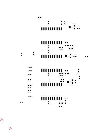
Note that the heat sinks have no solder mask with no paste, and that the thermal vias are present inside the heat sink pads.