Dec 15 2015
I am looking at this project after almost a year, trying to refresh my memory on how everything works. My task for today is to connect a heat sink to the thermal layer.
I checked the DipTrace website and found there was a minor update to version 2.4.0.2. I downloaded it and installed it on VS12 at D:\App\DipTrace\v242, leaving the v24 installation in place.
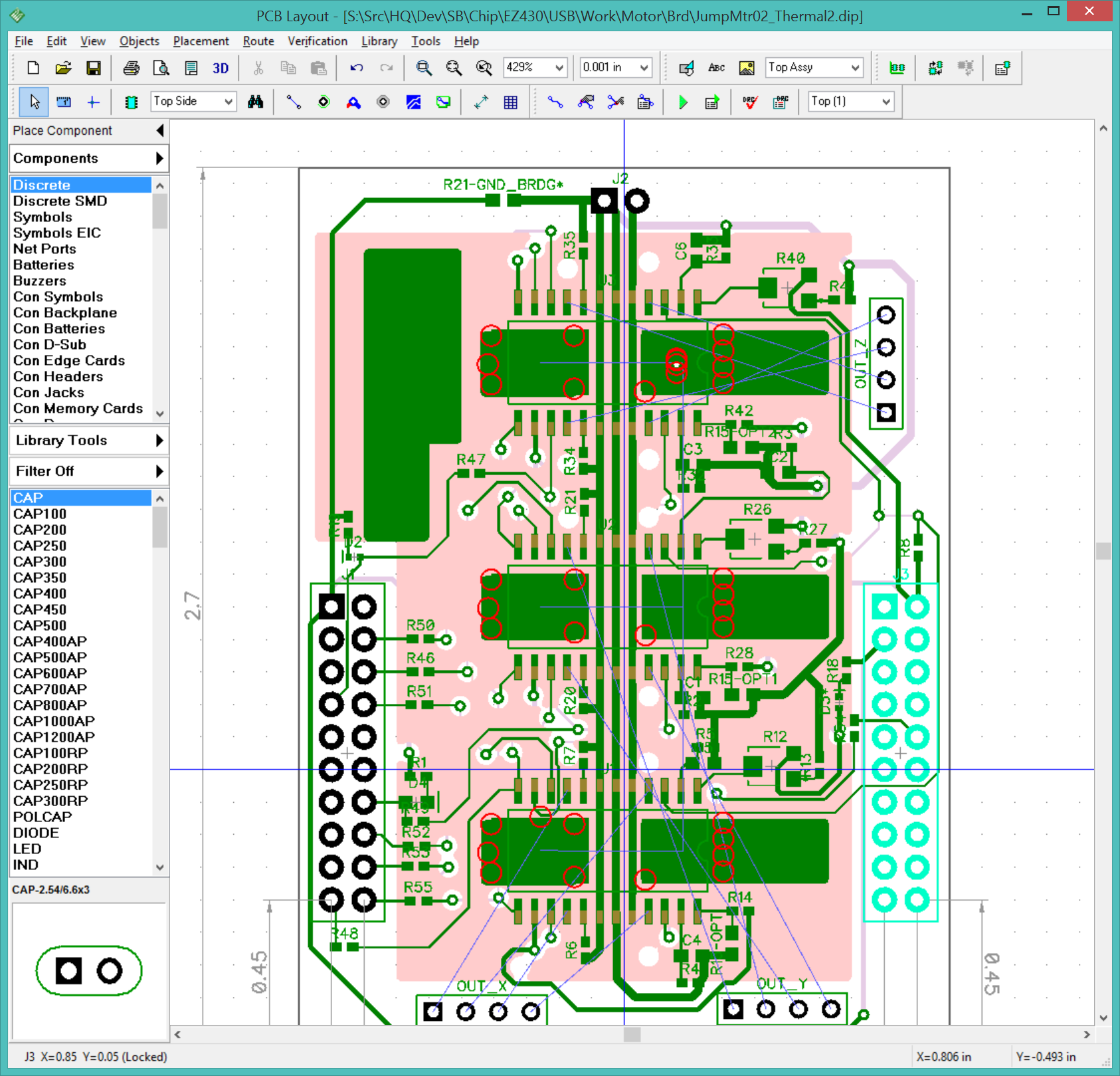
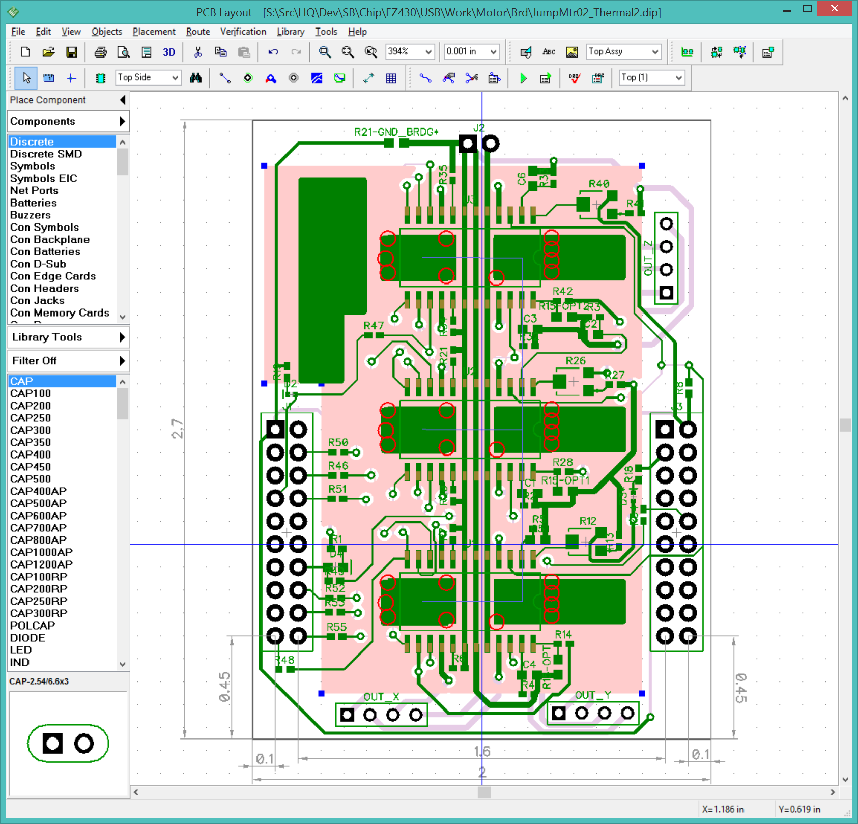
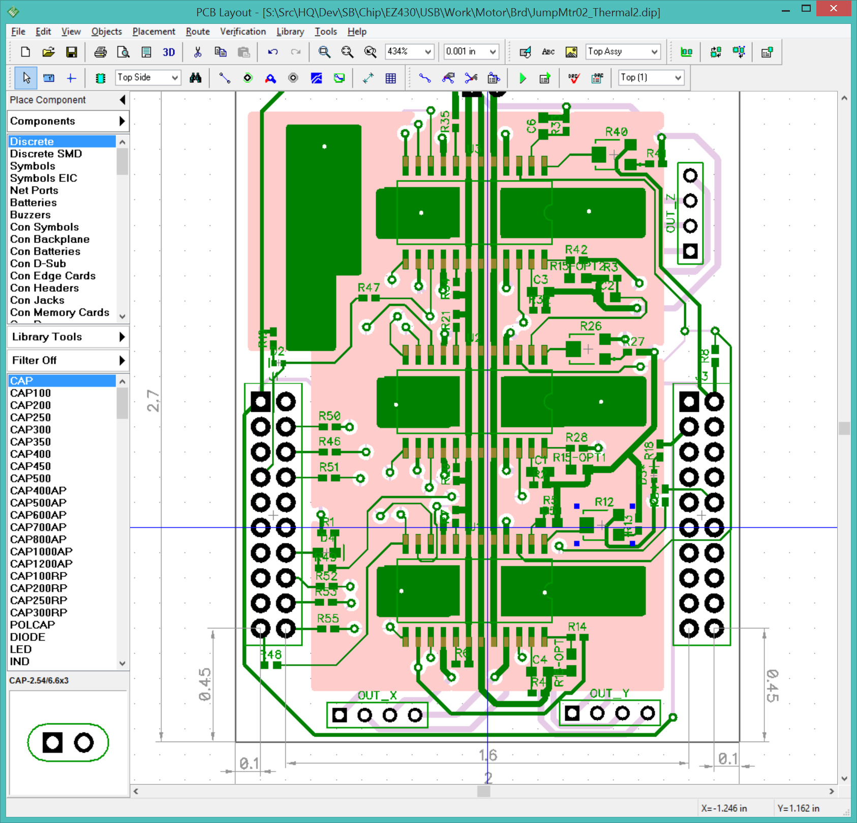
I created the copper pour for the heat sink and a static via to allow heat to flow from the IC into the thermal layer. DipTrace complains that the static via interferes with the copper pour on layer 1 because there is no net connecting them.
To make the connections between the components (the three driver ICs and the heat sink hardware) and the thermal layer (the copper pour) I need to create a thermal net. Just like an electrical net, this will let me connect together all the components to allow the heat to flow out of the ICs, into the copper pour of the thermal plane, then out through the heat sink into the environment.
I need to make sure there is a net to be connected in the schematic. I found that the schematic already has HEAT_X, HEAT_Y, and HEAT_Z nets. I renamed them to a common HEAT net so I could connect them to the same copper pour.
When I tried to renew from schematic, DipTrace complained that file did not exist. It has been moved to S:. I was able to update the related schematic using File > Design Information... > Related Schematic...
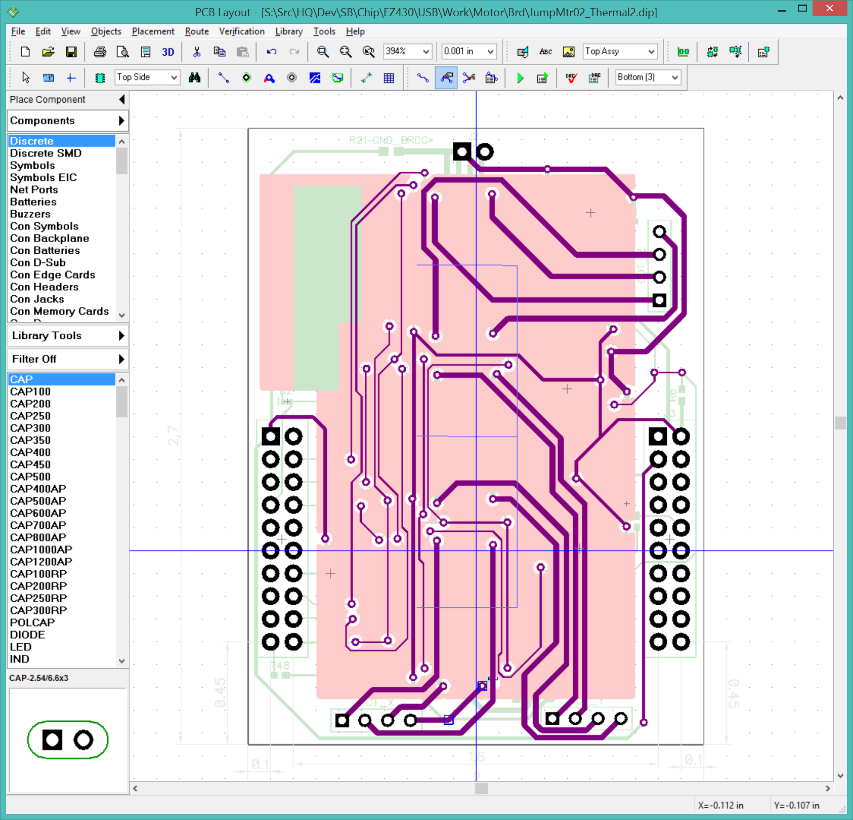
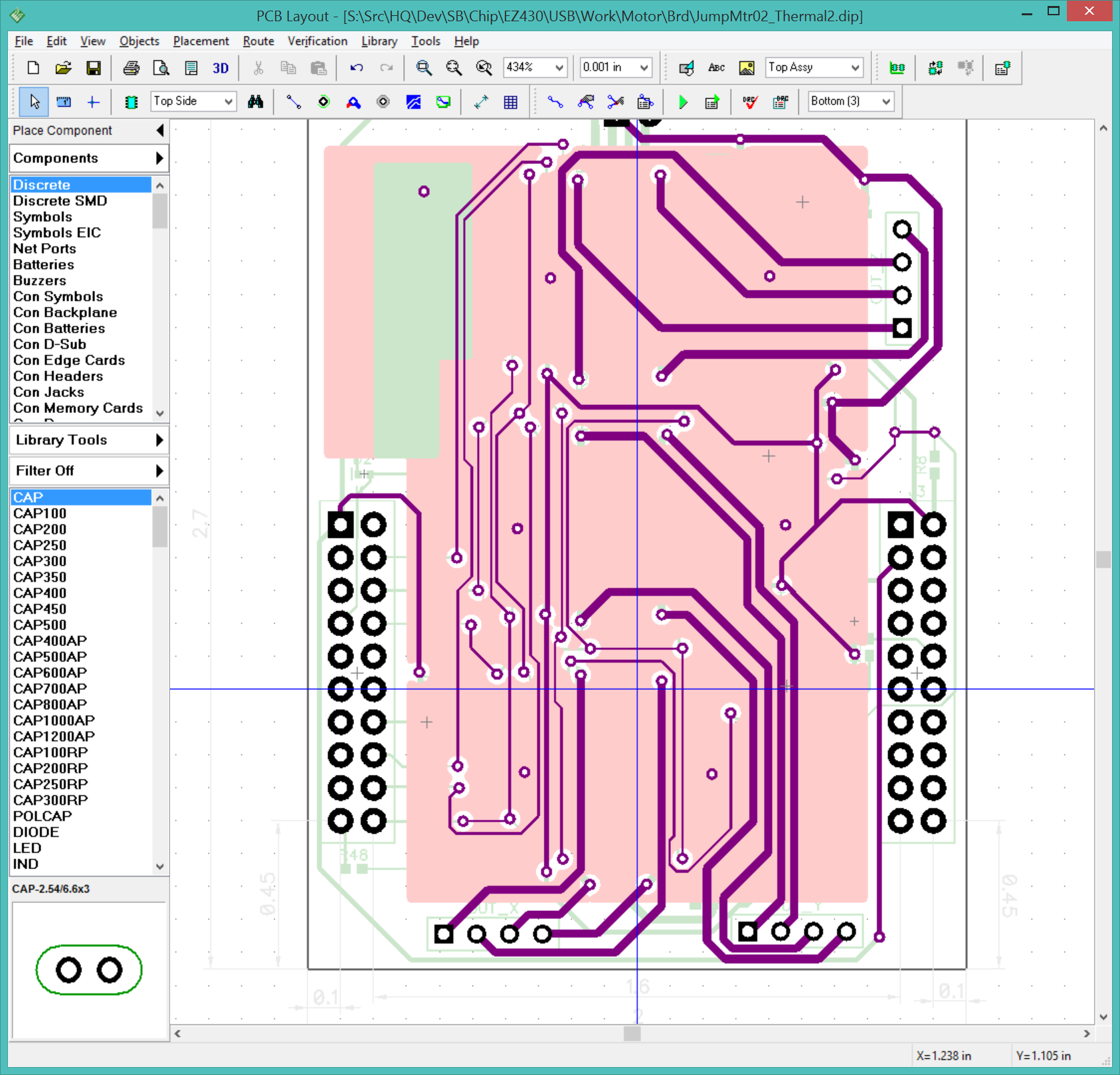
After the "renew from schematic" I found that the OUT_ pins were no longer connected. DipTrace had complained that the net class properties did not match between the schematic and the layout, and I selected "Use layout properties." Apparently, DipTrace removed the PWR_MTR traces from the layout. The voids in the thermal pour are still there where the PWR_MTR vias once were, providing hints on how to route them.
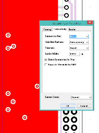
I updated the thermal pour after routing the PWR_MTR lines, then updated the properties of the pour to connect it to the HEAT net. The top layer pours under each motor driver IC is likewise added to the HEAT net as well as the pour under the heat sink. Static vias were then added inside the pours and connected to the HEAT net by right-click > Add to Net > Select from list > HEAT. A warning box will appear prompting to add the via to a different net if I accidentally drill through an existing trace. Click cancel, undo the via, and put it somewhere else. Once the HEAT net is fully connected using the static vias, I run the DRC verification until there are no errors. I visually confirm the HEAT connections, making sure there are no voids around my thermal vias inside the thermal pour (RED).
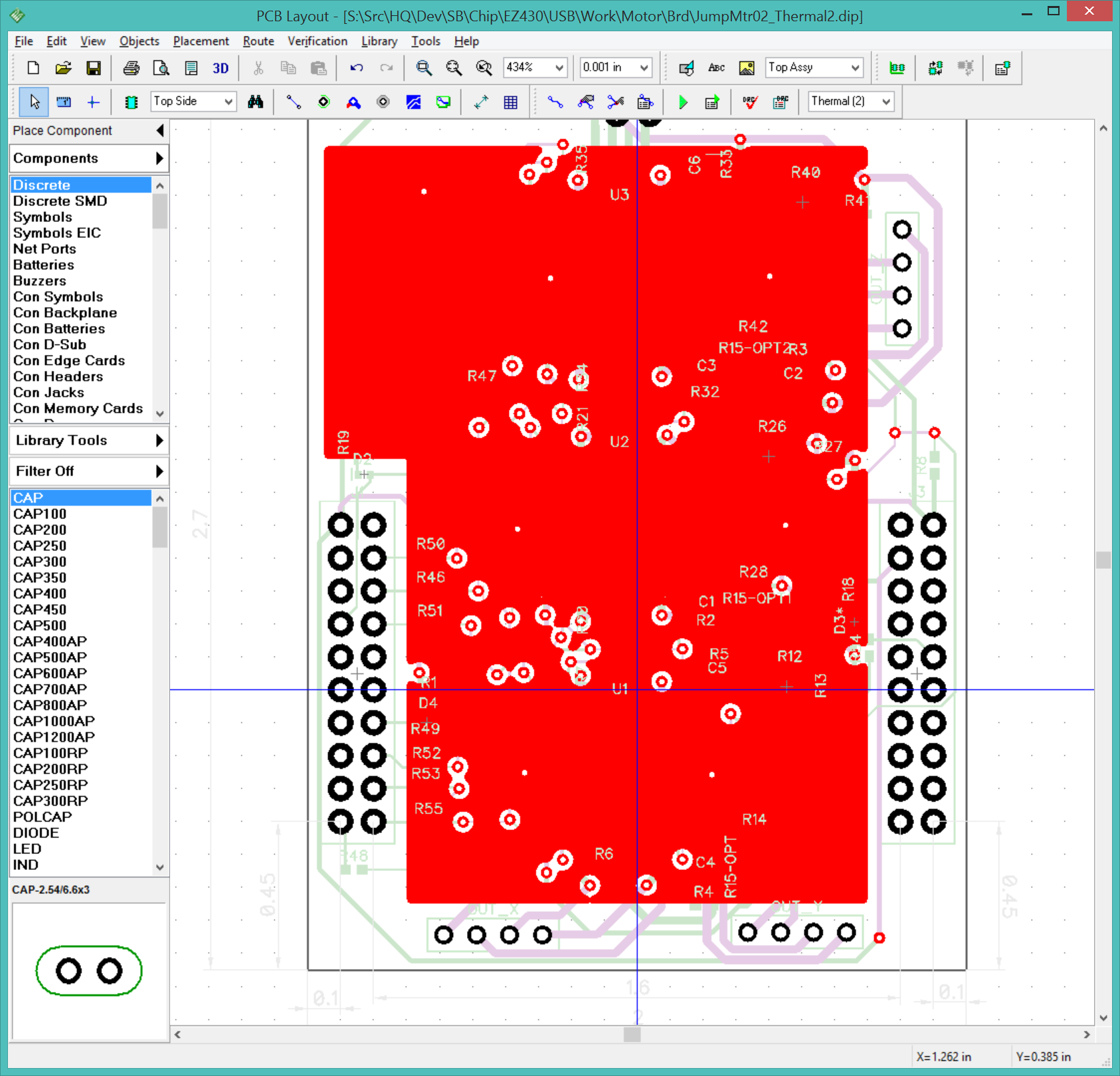
Thermal flow is improved by sprinkling more thermal vias around. Even though I don't intend to mount a heat sink, I added mounting holes just in case. Searching through Digikey revealed only 2(!) parts that would fit. Neither has mounting holes, I guess they are too small, and are mounted using adhesive. AE10817-ND is $0.92 for one, 501100B00000G-ND is $0.62 for one. Of course, this opens up the option of mounting heat sinks directly to the top of each driver IC. This would remove the need for a thermal layer on the board. The downside is having three heat sinks instead of one, they would be trickier to mount, and would extend further from the board surface. With the thermal plane there is a good chance a discrete heat sink would not be absolutely required.
The finished(?) board.

Gerber spec: [FILE 7050]
Circuit boards are fabricated by laminating one or more boards. Since each stratum has two sides, from a fabrication perspective there is no such thing as a "3-layer" board -- it is actually a 4-layer board. Restricting the design to three layers provides little or no cost savings over expanding it to four layers. In fact, adding a fourth layer will probably result in a smaller board as the routing is easier. However, a 4-layer board is roughly twice as expensive as a 2-layer board, and each additional layer pair increments the price by that same quantum step. A 6-layer board is 3X the cost of a 2-layer board.
Bottom line: Try to keep the number of layers to a minimum, as it makes a big difference in the cost of the design. If I do need an extra layer, add two.