September 7 2014 - Chip
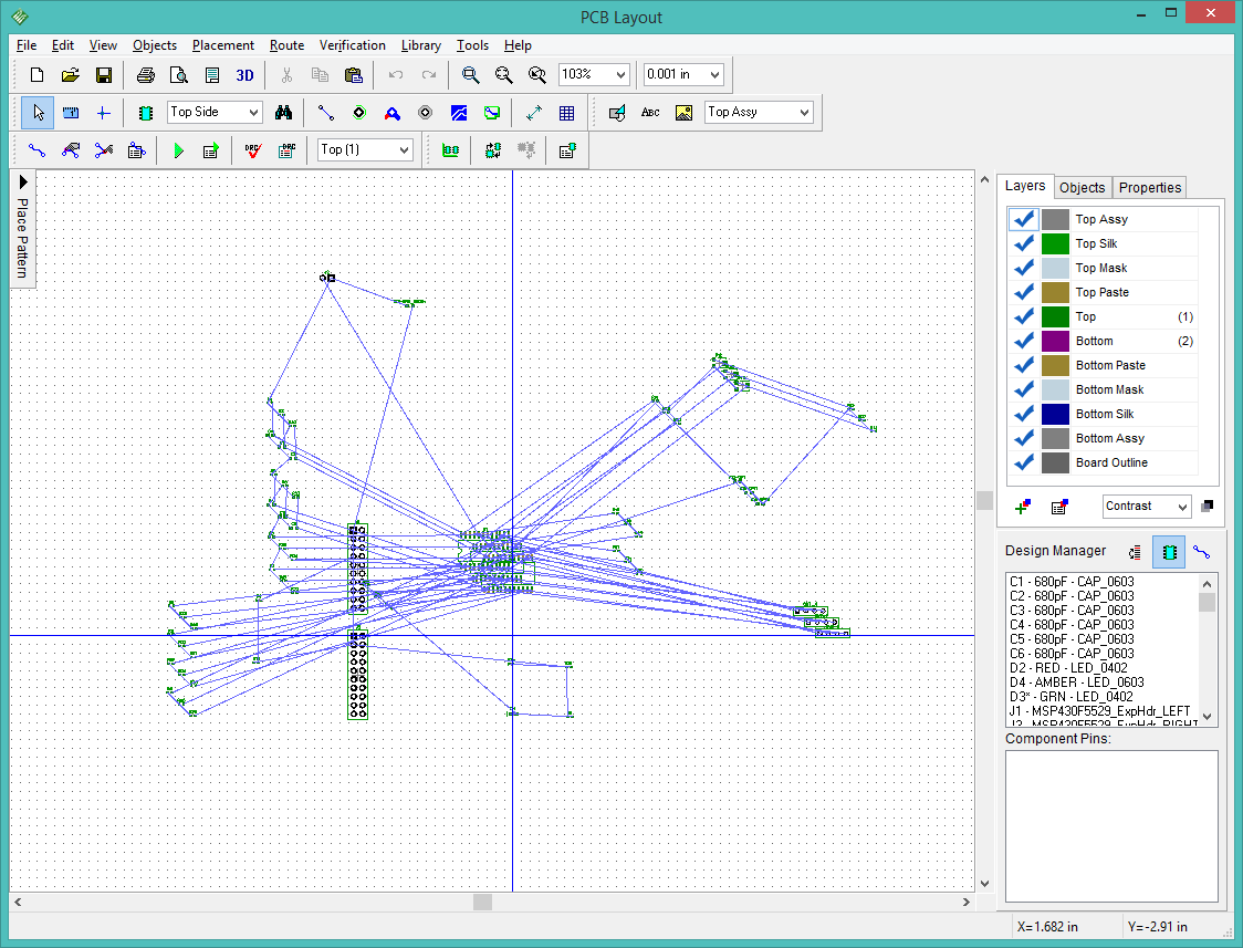
This is the initial layout from the schematic:
The first step is to deal with the physical constraints. In this
case, the only constraints are the locations of the two expansion
headers. The
TI Boosterpack pack page shows the location of the headers,
but does not include the dimensions of the overall board.
[ [FILE 7027] ]
I found a better page:
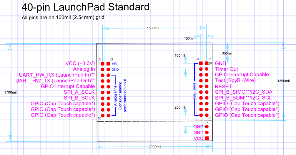
REMEMBER, I am placing my board on the bottom so the pins are flipped horizontally. The relative distances are the same.
The LaunchPad board is 2 1/4" by 2 7/8" (2.25 x 2.875). This puts the
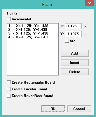
corners at ( -1.125, +1.4375 ). I create the board outline, with the
center at (0,0).
The two headers are 1800mil apart, outer row center to outer row center, and the outer rows are inset 100mil from the board edge. The top pin is (1700-350= 1350mil) from the bottom edge. This puts LEFT header pin 1 at (-1.125+0.100,-1.4375+1.350)= (-1.025,-0.0875). The offset to the center of the part is (+0.05,-0.445), so the part center is (-1.025+0.05,-0.0875-0.445) = (-0.975,-0.5325)
The RIGHT header pin 20 is then (-1.025+1.800,-0.0875) = (0.775,-0.0875). The offset to the part center is (-0.05,-0.445), so the center is (0.775-0.05,-0.0875-0.445)= (0.725,-0.5325)
Use the dimension markings to double-check the component locations. Once the headers are in the correct location, I select and lock them in place.
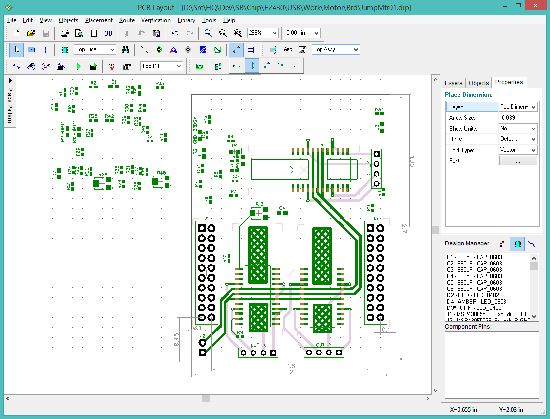
I copied the heat sinks from BlinkMtr02. This greatly increases the size of the footprint and makes it much more difficult to route but is necessary to disipate the heat. I routed the motor power lines, and space is already very cramped. This will be a difficult board to route.
I am reassessing my decision to mount the JumpMtr board on the underside facing out. I now believe it would be better to mount in on the underside facing up to make it stackable, then use right-angle jacks for the motor and external power connectors. Test points would be vias, accessible from the underside. If I decide this is better, I should make the change now before I invest a day or so working on the layout.
September 9 2014 - Chip
It became clear I was trying to stuff too many components onto too small a space. I looked at the schematic again and realized there were redundant resistors on each of the signal lines. I don't need a resistor for every motor driver input, only a single resistor on the MSP430 output is needed. This removed quite a few resistors, reducing the number of components to a more manageable number.

The silk markings on the board are there to help during the assembly/production phase. If the board is being assembled by a machine, the individual component markings are less important. The board would be much less cluttered if I had suppressed the "RefDes" markings. The really important markings are those that help the operator know if the board is oriented correctly and to help align the board in the machine. A "TOP" and "BOTTOM" label is very helpful. Headers should be well marked with a label for pin 1 that will be visible after the hardware is mounted. A version ID is very important, ideally with the date when the layout was submitted to the board fab. Battery posts should be labeled positive and negative.
I saved the new schematic as JumpMtr02.