September 3 2014 - Chip
The schematic is done. I am again surprised by how easy the schematic design comes together; it seems the devil is in the details of the layout.
The first step in the layout is to make sure every component used in the schematic has an associated pattern. Since I am reusing the BlinkMtr02 schematic, the only new part should be the expansion headers.
DipTrace handles components and patterns as completely separate things. I guess that makes sense as it breaks apart the function from the implementation. The schematic component holds the functional information: pins, electrical characteristic, and names. The pattern holds the implementation details: pad sizes and locations, and names. Separating function from pattern allows the circuit to be designed without being tied to a specific part. Parts from different manufacturers can be swapped in by assigning components to patterns. The names are the common item that ties a component to a pattern.
So the first step is to copy the reused patterns from the BlinkMtr02 library.
September 7 2014
The only new component pattern was the Expansion Header. The TI Booster pack uses a standard format of two 2x10 0.10" headers. I am placing my JumpMtr on the underside of the LaunchPad, which means I need to have male pins that will insert into the female header blocks. The board will have holes that will receive 2x10 headers, which will be soldered onto the JumpMtr board with the long ends extending downward from the bottom of the board toward the LaunchPad board.
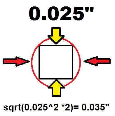
The dimensions of the male pins are:
0.025" square pin width
The holes for the header pins need to be larger and round. The theoretical size is 0.035" so I use 0.04" which seems to work well. Mark pin 1 with square on the silk.
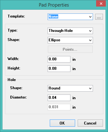
I launch DipTrace Pattern editor and open the JumpMtr.lib library and layout the expansion header, and add a new pattern. I set the default pad properties first.
The trick here is that the pins need to be numbered counter-clockwise from the upper left. I cannot use DipTrace's rectangular mode because it always places a top and bottom row (a bug IMHO), so I need to place 2 lines of 10 pins each. I want the pads placed precisely, so I use the Objects > Precise Pad Placement... dialog.
A couple notes:

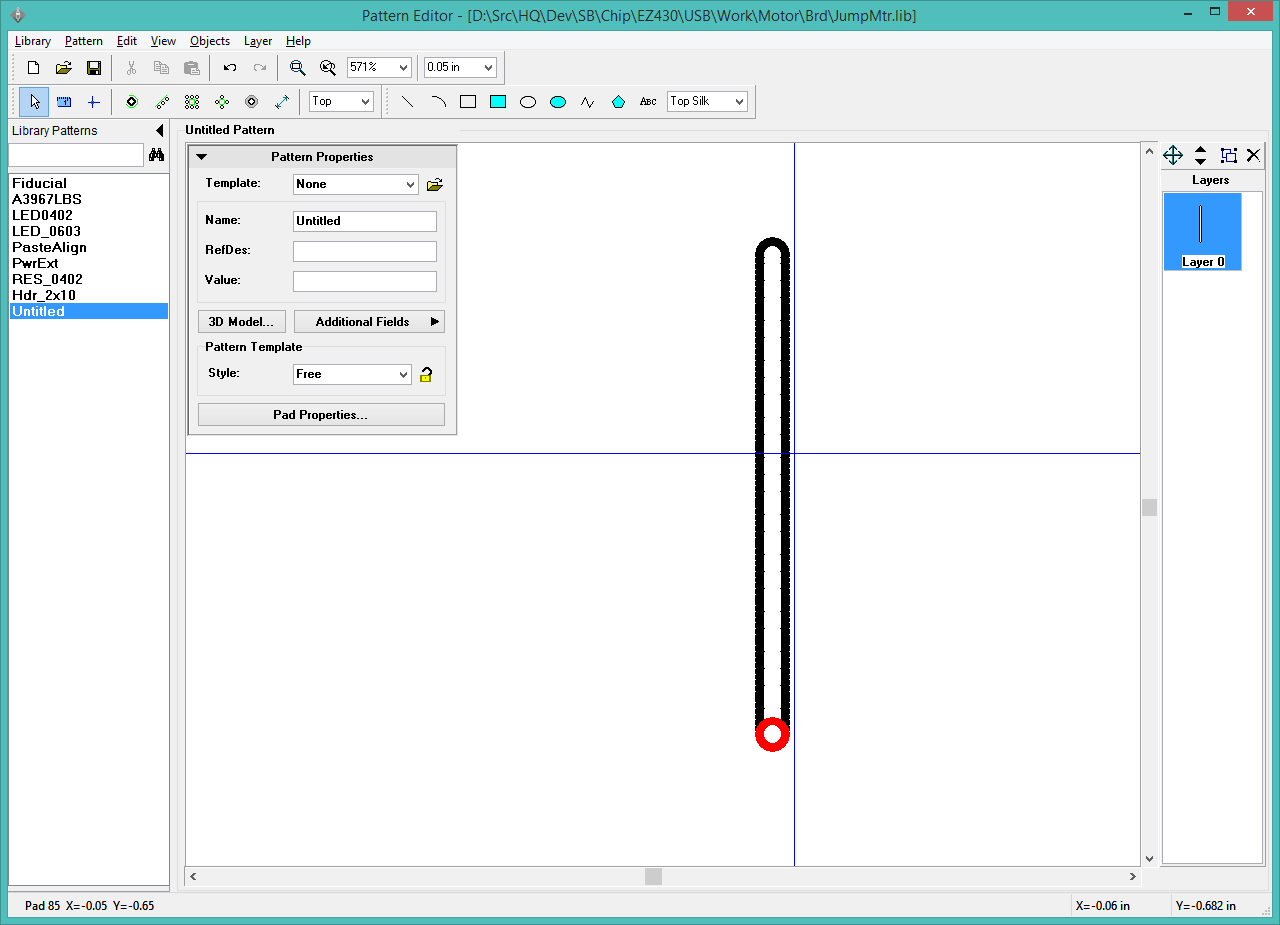
Well, that was not what I expected. Instead of placing a pad every -0.10" it seemed to calculate the start and end points correctly, but then placed 85 pads instead of 10. When I specify a positive value for Y spacing, it is correct but in the wrong order (pin 1 on the bottom). This seems to be a bug in DipTrace. The workaround is to place the line with pin 1 on the bottom, flip the component vertically, then add the second line.
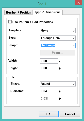
Finally, I want to change the silk for pin 1 from a circle to a rectangle. I select pin 1 and right-click "Properties...". I do not click the "Pad Properties..." button in the Pattern Properties box as this would change all the pads. I then uncheck "Use Pattern's Pad Properties" as I only want to change this single pin. Change the Shape from Ellipse to Rectangle and click OK.
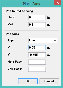
The second row is placed by setting the initial X to +0.05". Since I want this row to be numbered starting from the bottom it is placed correctly.
The final touch is to place a silk bounding box.
Save the library.
Now I need to attach the header pattern to the component. Launch DipTrace Component Editor and open JumpMtr.eli. Select the MSP430F5529_ExpHdr component. This component has two parts, LEFT and RIGHT; I need to attach the pattern to each part. Open the pin manager to make sure the pins are assigned correctly.
Save the component library.
Now I need to refresh the schematic by updating the component in the schematic. Launch DipTrace Schematic Capture and open JumpMtr01.dch. Select the "ExpHdr" page, select the J1.1 component, right-click "Update from Library > Selected Components".
Save the schematic.
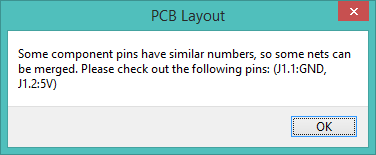
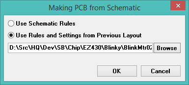
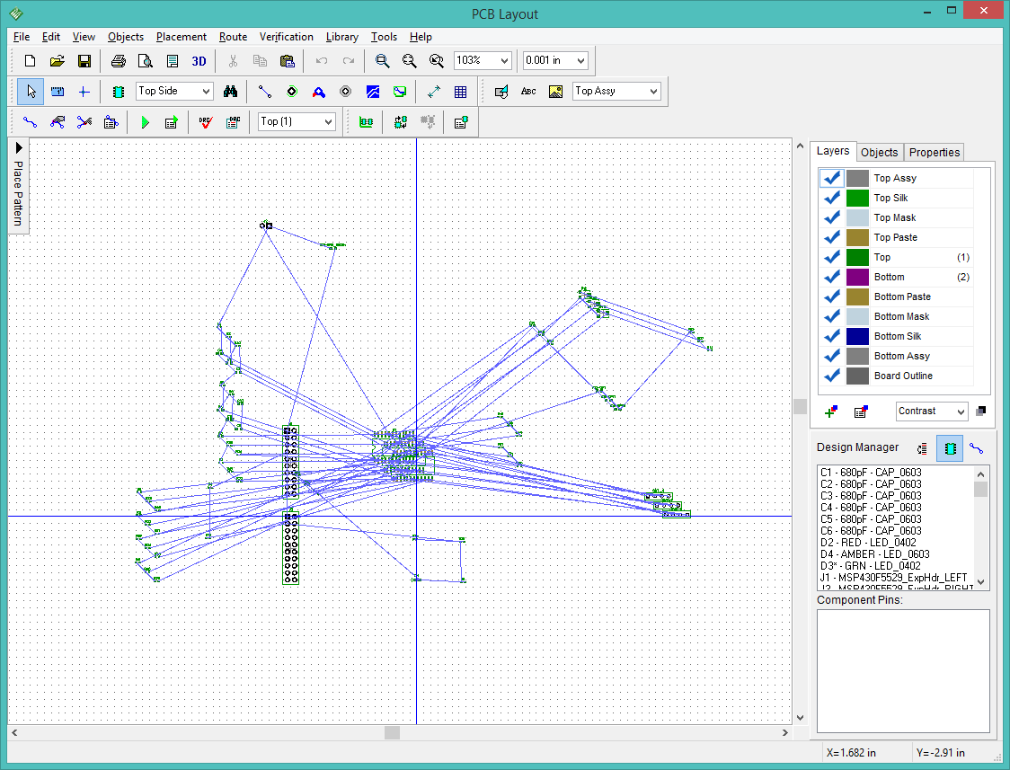
Now I want to perform a draft layout just to make sure the components look right. Click File > Convert to PCB. Let DipTrace merge nets.
I want to reuse my layout rules from the BlinkMtr02 project:
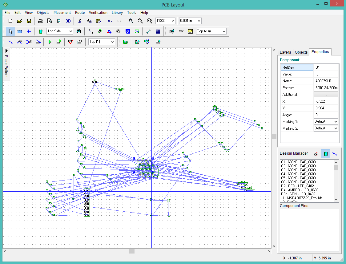
Here I run into my first problem. I created the expansion header in the Component library as a single component with two parts, but the layout only includes the LEFT part. The RIGHT header is missing.
I don't see anything wrong with the schematic, component, or part. This seems to be a DipTrace bug. The workaround seems to be: don't create multi-part components. I need to go back and create separate left and right header components. This changes the schematic and component libraries.
To split the two-part component into two separate components:
After replacing the header components (about 20 minutes), the draft layout looks better:
The moral of this lesson:
DipTrace multi-part components are broken, don't use them.
Next step is to position and route the layout components.