Now I hit my second major design decision: Assigning MSP430 pins to functions. The first step is to make a list of the JumpMtr functions I need. The MSP430 column is filled in later.
Existing Jumppad functions:
| JumpPad | MSP430 |
|---|---|
| S1 | P2.1 |
| S2 | P1.1 |
| LED1 RED | P1.0 |
| LED2 GRN | P4.7 |
New motor functions:
| JumpMtr | MSP430 | Remarks | |
|---|---|---|---|
| 1 | MTR_/RESET | P4.3 | Resets all drivers |
| 2 | MTR_ESTOP | P7.4 | Stops all drivers |
| 3 | MTR_MS1 | P8.1 | Driver step mode1, all axes |
| 4 | MTR_MS2 | P8.2 | Driver step mode2, all axes |
| 5 | MTR_DIR_X | P1.6 | Driver1 direction |
| 6 | MTR_STEP_X | P1.4 | Driver1 step |
| 7 | MTR_DIR_Y | P3.7 | Driver2 direction |
| 8 | MTR_STEP_Y | P1.5 | Driver2 step |
| 9 | MTR_DIR_Z | P4.0 | Driver3 direction |
| 10 | MTR_STEP_Z | P2.4 | Driver3 step |
The second step is to make a list of the available pins and fill in any pre-assigned functions. I only need to worry about pins that are included in the expansion headers. This is the pinout for the expansion header as viewed from the bottom, counter-clockwise from the upper left:
LEFT
| LaunchPad Pin | MSP430 | JumpMtr |
|---|---|---|
| L01 | GND | GND |
| L02 | P2.0 | |
| L03 | P2.2 | |
| L04 | P7.4 | MTR_ESTOP |
| L05 | RST | |
| L06 | P3.0 | |
| L07 | P3.1 | |
| L08 | P2.6 | |
| L09 | P2.3 | |
| L10 | P8.1 | MTR_MS1 |
| LaunchPad Pin | MSP430 | JumpMtr |
|---|---|---|
| L20 | P2.5 | |
| L19 | P2.4 | MTR_STEP_Z |
| L18 | P1.5 | MTR_STEP_Y |
| L17 | P1.4 | MTR_STEP_X |
| L16 | P1.3 | |
| L15 | P1.2 | |
| L14 | P4.3 | MTR_/RESET |
| L13 | P4.0 | MTR_DIR_Z |
| L12 | P3.7 | MTR_DIR_Y |
| L11 | P8.2 | MTR_MS2 |
RIGHT
| LaunchPad Pin | MSP430 | JumpMtr |
|---|---|---|
| R01 | 5V | 5V |
| R02 | GND | GND |
| R03 | P6.0 | STALL_X |
| R04 | P6.1 | STALL_Y |
| R05 | P6.2 | STALL_Z |
| R06 | P6.3 | |
| R07 | P6.4 | |
| R08 | P7.0 | |
| R09 | P3.6 | |
| R10 | P3.5 |
| LaunchPad Pin | MSP430 | JumpMtr |
|---|---|---|
| R20 | 3V3 | 3V3 |
| R19 | P6.5 | |
| R18 | P3.4 | |
| R17 | P3.3 | |
| R16 | P1.6 | MTR_DIR_X |
| R15 | P6.6 | |
| R14 | P3.2 | |
| R13 | P2.7 | |
| R12 | P4.2 | |
| R11 | P4.1 |
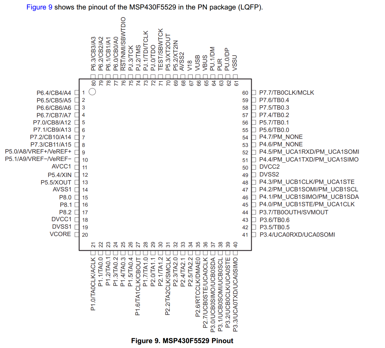
The pinout for the MSP430 package is useful for looking up the MSP430 pin numbers.
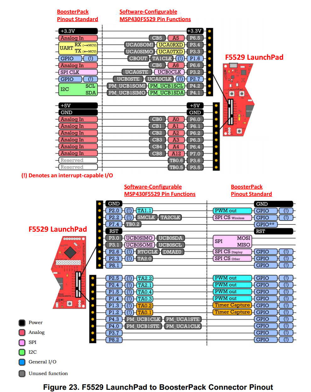
This figure is useful for determining which functions are available on the expansion headers. It also lists the "standard" usage for BoosterPacks. It is good to adhere to the standard uses when possible, this allows boards to be stacked.
I need to look up all the pins on the MSP430F5529 to fill out the table, which will also be used later to create the MSP430F5529 component. This table includes the pin name (primary function), MSP430 package pin number, function list, standard BoosterPack usage, and a (initially) blank column for the JumpMtr usage.
| Name | Pin | MSP430 | Std | JumpMtr | Remarks |
|---|---|---|---|---|---|
| RST | 76 | !RST/NMI/SBWTDIO | |||
| P1.2 | 23 | P1.2/TA0.0 | Timer Capture | ||
| P1.3 | 24 | P1.3/TA0.2 | Timer Capture | ||
| P1.4 | 25 | P1.4/TA0.3 | PWM out | MTR_STEP_X | |
| P1.5 | 26 | P1.5/TA0.4 | PWM out | MTR_STEP_Y | |
| P1.6 | 27 | P1.6/TA1CLK/CBOUT | GPIO | MTR_DIR_X | |
| P2.0 | 29 | P2.0/TA1.1 | PWM out | ||
| P2.2 | 31 | P2.2/TA2CLK/SMCLK | SPICS (wireless) | ||
| P2.3 | 32 | P2.3/TA2.0 | SPICS (other) | ||
| P2.4 | 33 | P2.4/TA2.1 | PWM out | MTR_STEP_Z | |
| P2.5 | 34 | P2.5/TA2.2 | PWM out | ||
| P2.6 | 35 | P2.6/RTCCLK/DMAE0 | SPICS (display) | ||
| P2.7 | 36 | P2.7/UCB0STE/UCA0CLK | GPIO | ||
| P3.0 | 37 | P3.0/UCB0SIMO/UCB0SDA | SPIMOSI | ||
| P3.1 | 38 | P3.1/UCB0SOMI/UCB0SCL | SPIMISO | ||
| P3.2 | 39 | P3.2/UCB0CLK/UCA0STE | SPICLK | ||
| P3.3 | 40 | P3.3/UCA0TXD/UCA0SIMO | UART/TX | ||
| P3.4 | 41 | P3.4/UCA0RXD/UCA0SOMI | UART/RX | ||
| P3.5 | 42 | P3.5/TB0.5 | RESERVED | ||
| P3.6 | 43 | P3.6/TB0.6 | RESERVED | ||
| P3.7 | 44 | P3.7/TB0OUTH/SVMOUT | GPIO | MTR_DIR_Y | |
| P4.0 | 45 | P4.0/PM_UCB1STE/PM_UCA1CLK | GPIO | MTR_DIR_Z | |
| P4.1 | 46 | P4.1/PM_UCB1SIMO/PM_UCB1SDA | I2CSDA | ||
| P4.2 | 47 | P4.2/PM_UCB1SOMI/PM_UCB1SCL | I2CSCL | ||
| P4.3 | 48 | P4.3/PM_UCB1CLK/PM_UCA1STE | GPIO | MTR_/RESET | |
| P6.0 | 77 | P6.0/CB0/A0 | Analog In | RESERVED: STALL_X | |
| P6.1 | 78 | P6.1/CB1/A1 | Analog In | RESERVED: STALL_Y | |
| P6.2 | 79 | P6.2/CB2/A2 | Analog In | RESERVED: STALL_Z | |
| P6.3 | 80 | P6.3/CB3/A3 | Analog In | RESERVED | |
| P6.4 | 01 | P6.4/CB4/A4 | Analog In | RESERVED | |
| P6.5 | 02 | P6.5/CB5/A5 | Analog In | ||
| P6.6 | 03 | P6.6/CB6/A6 | Analog In | ||
| P7.0 | 05 | P7.0/CB8/A12 | Analog In | ||
| P7.4 | 57 | P7.4/TB0.2 | GPIO | MTR_ESTOP | |
| P8.1 | 16 | P8.1 | GPIO | MTR_MS1 | |
| P8.2 | 17 | P8.2 | GPIO | MTR_MS2 |
I want to use PWM outputs to drive the steps, so I will assign P1.4/TA0.3 to MTR_STEP_X, P1.5/TA0.4 to MTR_STEP_Y, and P2.4/TA2.1 to MTR_STEP_Z.
I want to keep the analog inputs available for future use, so pins P6.0-6 and P7.0 are reserved. The next revision will use the analog inputs to monitor current draw through the motors to detect stalls.
I need 2 GPIO outputs on the same port for MTR_MS1 and MTR_MS2; P8.1-2 are the only GPIO pins that are together.
Now I just fill in the GPIO pins with MTR_DIR_X/Y/Z, MTR_/RESET, and MTR_ESTOP: P1.6, P3.7, P4.0, P4.3, and P7.4
I fill these assignments into both tables, as they are both useful. Double and triple-check, and the pin assignment is done.
Wow! That was a lot of work! Assigning the pins while constantly updating the pages and tables has taken about five hours. I will finish the ExpHdr page of the schematic and stop. I have a lot of work to do for my day job tomorrow.
The schematic was easier than expected, I was able to finish the first draft of the entire board in just another 30 minutes. The schematic is quite simple, just the expansion headers, three indicator leds, and three instances of the A3967SLB circuit.