April 15 2016
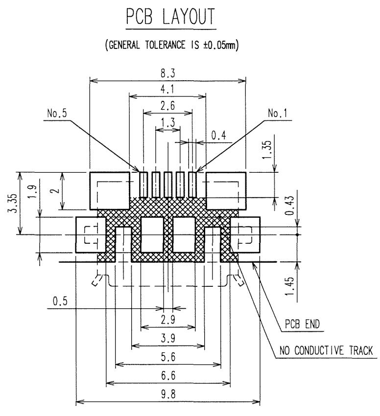
The microUSB connector on the LaunchPad uses the Hirose ZX62R-B-5P (Digikey H11574CT-ND). The datasheet is typical: all the information is there, just not in a form that is easy to use. Is it so hard to simply provide a table listing all the pads by Center(x,y) and area(W,H)? Instead I have to reinterpret the geometry to create the pads. Not difficult, just tedious and error-prone.
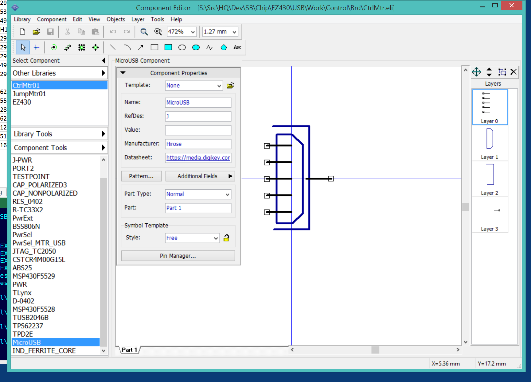
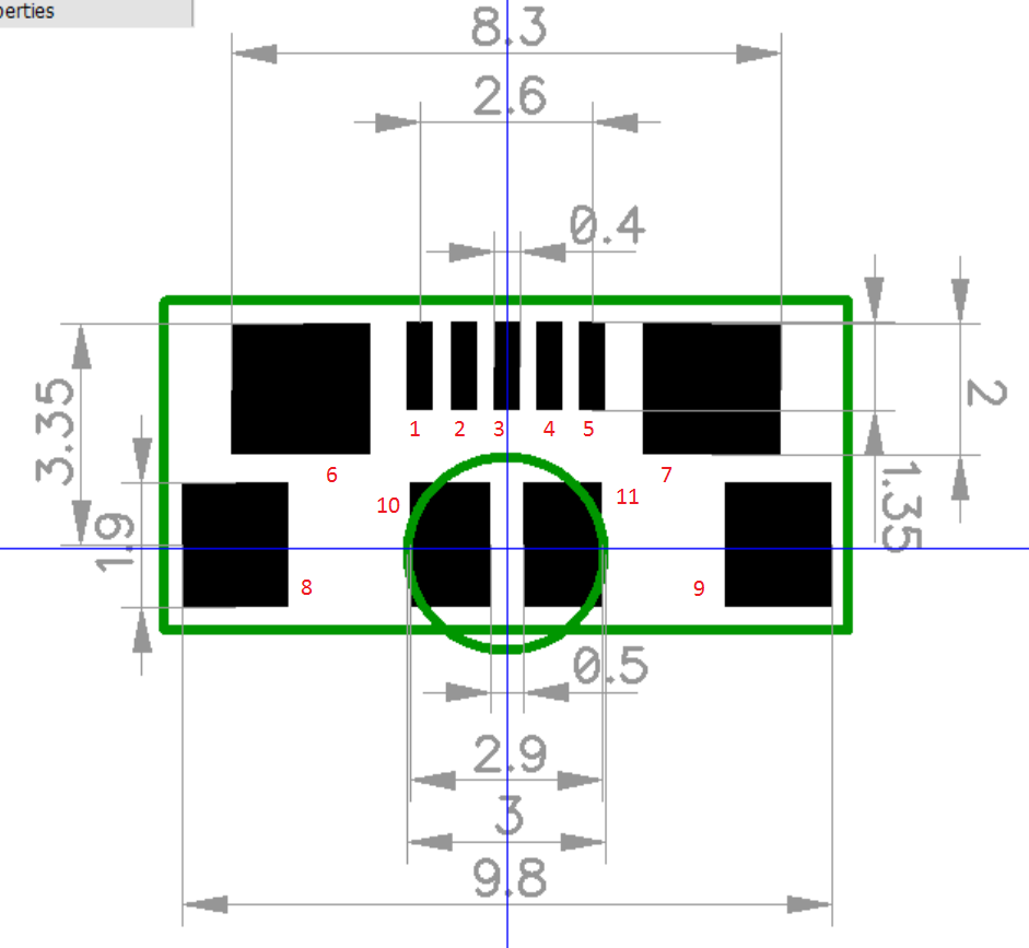
After the pads are placed and I have double-checked the dimensions against the datasheet drawing, I need to move the origin to the pick point on the part. The "picking area" is indicated by the circle. The circle will generate a "silk over pad" DRC error; this can either be ignored or solved by deleting the circle after placing the component on the board.
Having this table would have saved me at least an hour.
| Pad | Center | WxH |
|---|---|---|
| 1 | (-1.30, 2.75) | 0.40x1.35 |
| 2 | (-0.65, 2.75) | 0.40x1.35 |
| 3 | ( 0.00, 2.75) | 0.40x1.35 |
| 4 | ( 0.65, 2.75) | 0.40x1.35 |
| 5 | ( 1.30, 2.75) | 0.40x1.35 |
| 6 | (-3.10, 2.40) | 2.10x2.00 |
| 7 | ( 3.10, 2.40) | 2.10x2.00 |
| 8 | (-4.10, 0.05) | 1.60x1.90 |
| 9 | ( 4.10, 0.05) | 1.60x1.90 |
| 10 | (-0.85, 0.05) | 1.20x1.90 |
| 11 | ( 0.85, 0.05) | 1.20x1.90 |
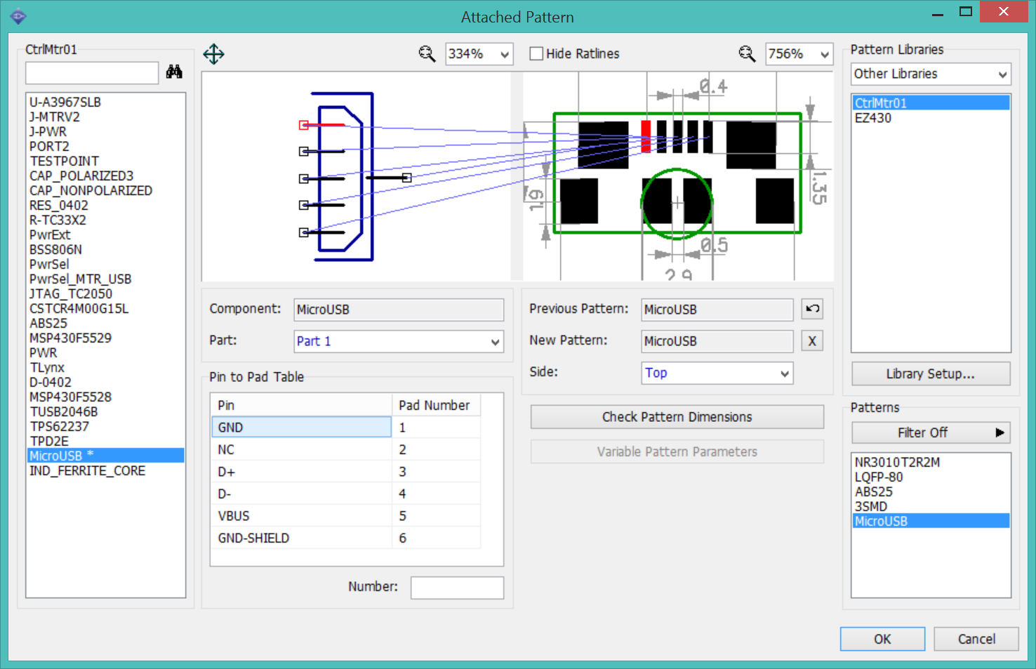
There is a nagging doubt about whether Pin1 and Pad1 are properly connected. The Hirose datasheet does not concern itself with signals. I am also troubled by the "R" in the part number, which may indicate "Reversed". This needs to be checked before layout.