Sunday May 10 2014
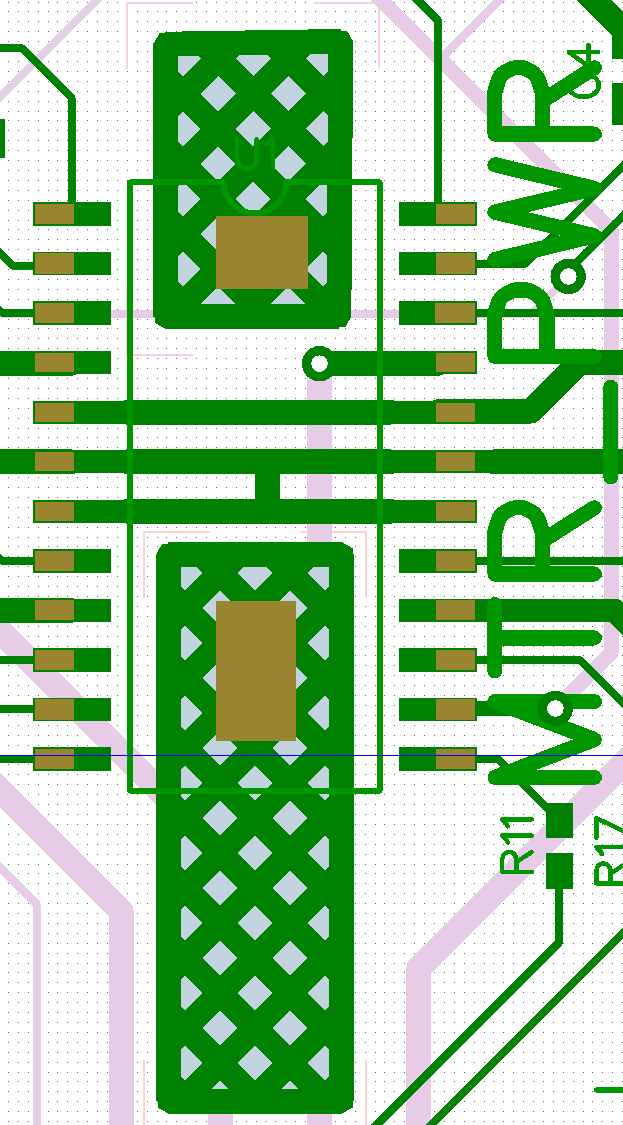
I added a heat sink in the form of a copper pour under the A3967, which included a couple twists. First, there are 2 pairs of ground pins on each side of the IC. This made a single heat sink impractical as it would mean routing a thick MTR_PWR ground trace to circumnavigate the IC. Second, the copper pour is isolated from the IC without some sort of net connection. I solved this by adding a custom shape to the solder mask (but not the solder paste) layer over the copper pours. I did not want to completely fill the area with solder paste because solder is not a good heat conductor (better than air, worse than copper) and I did not want a huge glob of solder between the IC and the board. So I added a smaller custom shape to the solder paste layer to provide some connectivity without filling the entire area. This approach may fail if the solder thins across the entire solder mask void so that it no longer makes contact with the IC, creating an air bridge that will reduce the heat dissipation. If this happens, I will need to remove the solder paste shape then manually fill the void with heat paste before placing the components. Hopefully this will not be necessary.
All the heat sink work was done in Layout, so it will need to be recreated for every instance of the A3967. It would be better if the heat sink shapes could be added to the component pattern, but I did not see how to do it. I should revisit this later.
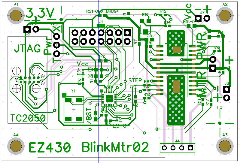
This change also prompted me to flip the orientation of the A3967, which caused the layout to diverge so far from the BlinkMtr01 layout that it was easier to restart the layout from scratch. I knew I also had to reroute all the TC2050 connections, so this was an easy decision.
I addressed the issues from the BlinkMtr01 post-mortem, and added test points for both 3.3V Vcc and MTR_PWR. I also brought all the unused MSP430 ports out to vias (inadvertently including a couple NC pins). This would allow me to put a scope on the ports even if they were not connected to anything. Laying out the new BlinkMtr02 board took about six hours, most of Sunday afternoon and a bit of Monday.
I submitted the boards to Bay Area Circuits on Tuesday, $77.24 for 5 boards. Now that I am familiar with how BAC works, I like using them. They are a bit slow, a "5 day turn" really means 2 weeks, making the boards the long pole in every build. But the quality of the boards is very good and they will include bonus boards if there is unused space on their panel. The number of bonus boards is completely random, and may be zero, but this is better than the other shops where the number of bonus boards is always zero. I receive a lot of spam from Sunstone for their "ValueProto" boards. I must be missing something, because a Sunstone board "as low as" $28 is still more than twice as expensive as a "Deluxe" board from BAC at around $10.
I ordered a BlinkMtr02 stencil from OHaraRP.com for $27. I am now comfortable using the klapton stencils, with 100% success for the last 8 or so boards.
I ordered more MSP430s (25 @ $3.36) and A3967s (20 @ $3.15) to make sure I won't run out.
The BlinkMtr02 boards should arrive next Thursday or Friday. I will need to create a new BlinkMtr02 PnP project -- that can wait until Tuesday or Wednesday. I won't need to load any autofeeders, just export the PnP table from DipTrace and run it through ACAD. It should not take more than an hour and another hour for a production test run on a paper board.
If BlinkMtr02 comes to life without any major problems, the next step will be BlinkMtr03...