2016-04-08 19:34:56 chip
Page 1638
📢 PUBLIC
April 7 2016
09:50> The motor controller inputs need to be connected to the
Control MSP430 using the same pin assignments from the JumpMtr02
project. I copy the pin assignment table from {THREAD_LINK:1238}.
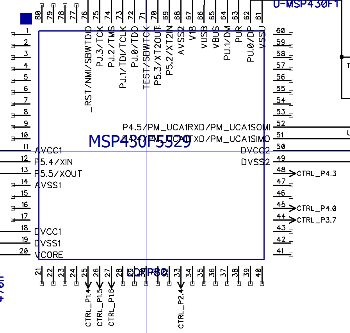
| Name | Pin | MSP430 | Std | CtrlMtr | Remarks |
|---|
| RST | 76 | !RST/NMI/SBWTDIO | | | |
| P1.0 | 21 | P1.0 | | J641.4 | |
| P1.1 | 22 | P1.1 | | J641.5 | |
| P1.2 | 23 | P1.2/TA0.0 | | RED, J641.6 | |
| P1.3 | 24 | P1.3/TA0.2 | | GRN, J641.7 | |
| P1.4 | 25 | P1.4/TA0.3 | PWM out | MTR_STEP_X, J641.8 | |
| P1.5 | 26 | P1.5/TA0.4 | PWM out | J641.9 | |
| P1.6 | 27 | P1.6/TA1CLK/CBOUT | GPIO | MTR_DIR_X, J641.10 | |
| P2.0 | 29 | P2.0/TA1.1 | PWM out | MTR_STEP_Y, J641.12 | |
| P2.1 | 30 | P2.1/TA1.2 | PWM out | MCP25625 /CS, J641.13 | |
| P2.2 | 31 | P2.2/TA2CLK/SMCLK | SPICS (wireless) | J641.14 | |
| P2.3 | 32 | P2.3/TA2.0 | SPICS (other) | J641.15 | |
| P2.4 | 33 | P2.4/TA2.1 | PWM out | MTR_STEP_Z, J641.16 | |
| P2.5 | 34 | P2.5/TA2.2 | PWM out | J641.17 | |
| P2.6 | 35 | P2.6/RTCCLK/DMAE0 | SPICS (display) | J641.18 | |
| P2.7 | 36 | P2.7/UCB0STE/UCA0CLK | GPIO | J641.19 | |
| P3.0 | 37 | P3.0/UCB0SIMO/UCB0SDA | SPIMOSI | CTRL_MOSI | |
| P3.1 | 38 | P3.1/UCB0SOMI/UCB0SCL | SPIMISO | CTRL_MISO | |
| P3.2 | 39 | P3.2/UCB0CLK/UCA0STE | SPICLK | CTRL_SCK | |
| P3.3 | 40 | P3.3/UCA0TXD/UCA0SIMO | UART/TX | | |
| P3.4 | 41 | P3.4/UCA0RXD/UCA0SOMI | UART/RX | | |
| P3.5 | 42 | P3.5/TB0.5 | GPIO | MTR_/SLEEP | |
| P3.6 | 43 | P3.6/TB0.6 | RESERVED | | |
| P3.7 | 44 | P3.7/TB0OUTH/SVMOUT | GPIO | MTR_DIR_Y | |
| P4.0 | 45 | P4.0/PM_UCB1STE/PM_UCA1CLK | GPIO | MTR_DIR_Z | |
| P4.1 | 46 | P4.1/PM_UCB1SIMO/PM_UCB1SDA | I2CSDA | | |
| P4.2 | 47 | P4.2/PM_UCB1SOMI/PM_UCB1SCL | I2CSCL | | |
| P4.3 | 48 | P4.3/PM_UCB1CLK/PM_UCA1STE | GPIO | MTR_/RESET | |
| P6.0 | 77 | P6.0/CB0/A0 | Analog In | RESERVED: STALL_X | |
| P6.1 | 78 | P6.1/CB1/A1 | Analog In | RESERVED: STALL_Y | |
| P6.2 | 79 | P6.2/CB2/A2 | Analog In | RESERVED: STALL_Z | |
| P6.3 | 80 | P6.3/CB3/A3 | Analog In | RESERVED | |
| P6.4 | 01 | P6.4/CB4/A4 | Analog In | RESERVED | |
| P6.5 | 02 | P6.5/CB5/A5 | Analog In | | |
| P6.6 | 03 | P6.6/CB6/A6 | Analog In | | |
| P7.0 | 05 | P7.0/CB8/A12 | Analog In | | |
| P8.0 | 15 | P8.0 | GPIO | MTR_ESTOP /ENABLE, J641.20 | |
| P8.1 | 16 | P8.1 | GPIO | MTR_MS1 | |
| P8.2 | 17 | P8.2 | GPIO | MTR_MS2 | |
I want to be able to drive all three motors using PWM outputs at
different frequencies. This requires changing MTR_STEP_Y from P1.5,
which shares TA0 with MTR_STEP_X, to P2.1 (TA1). Avoid using TXn.0
pins, as these cannot be used to generate variable-width pulses.
Expansion Header
| J641 Pin | Signal | CtrlMtr |
|---|
| 1 | GND | |
| 2 | VCC_5V | |
| 3 | VCC_3V | |
| 4 | CTRL_P1.0 | |
| 5 | CTRL_P1.1 | |
| 6 | CTRL_P1.2 | RED |
| 7 | CTRL_P1.3 | GRN |
| 8 | CTRL_P1.4 | MTR_STEP_X |
| 9 | CTRL_P1.5 | |
| 10 | CTRL_P1.6 | MTR_DIR_X |
| 11 | -- | |
| 12 | CTRL_P2.0 | MTR_STEP_Y |
| 13 | CTRL_P2.1 | |
| 14 | CTRL_P2.2 | |
| 15 | CTRL_P2.3 | |
| 16 | CTRL_P2.4 | MTR_STEP_Z |
| 17 | CTRL_P2.5 | |
| 18 | CTRL_P2.6 | |
| 19 | CTRL_P2.7 | |
| 20 | CTRL_P8.0 | ESTOP |
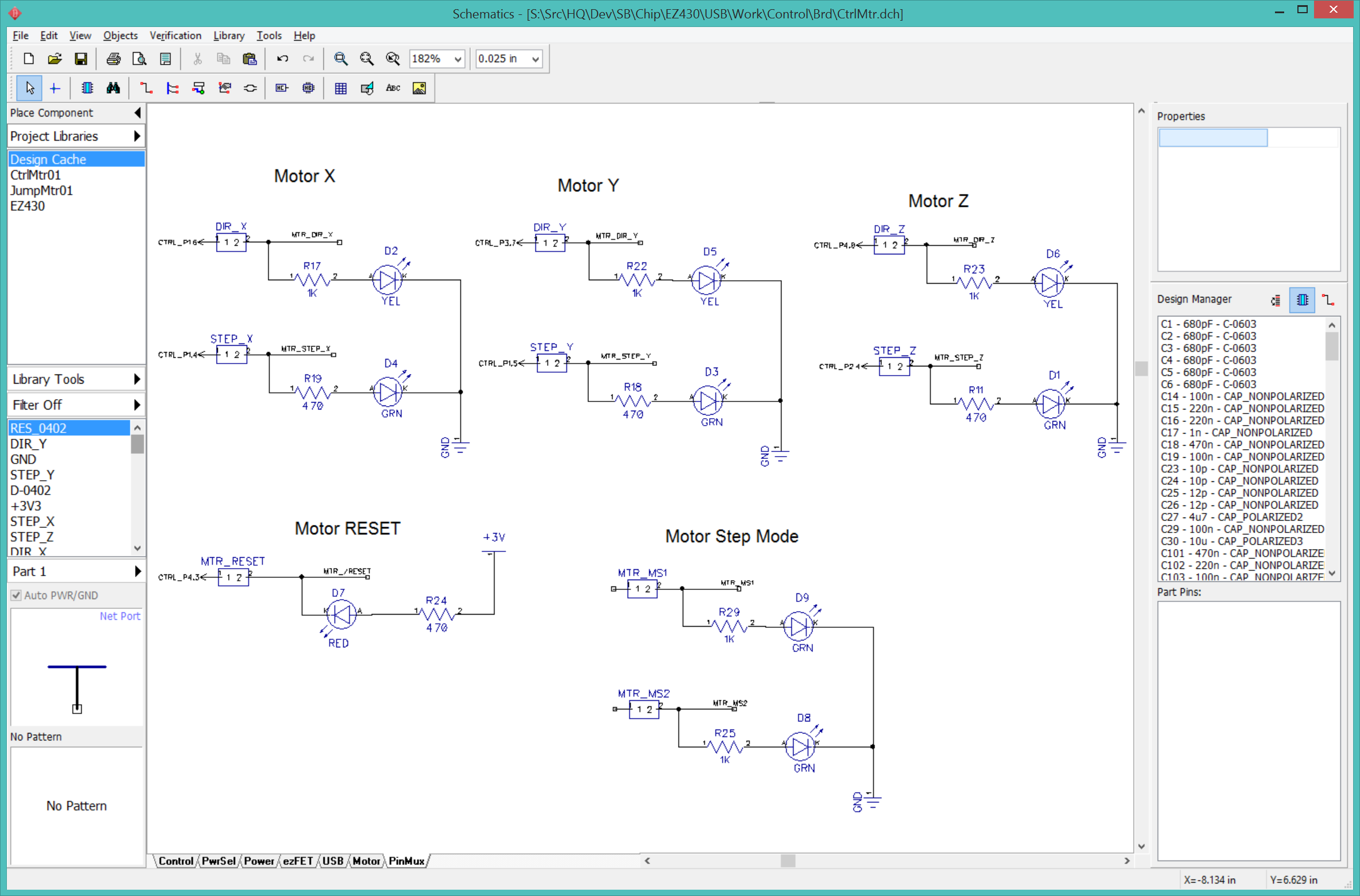
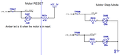
ESTOP
Emergency stop (ESTOP) is implemented as a signal connected to
/ENABLE on all motor drivers. This line is normally pulled low by a
100K pull-down (R610) and is connected to the expansion header J641
pin 20. This can be connected to an external normally open switch
between J641.3 (VCC_3V) and J641.20 (MTR_ESTOP). MTR_ESTOP is
connected to 5528 P8.0, which should normally be configured as an
input to detect an ESTOP condition, or configured as an output to
simulate an ESTOP. ESTOP is indicated by the red led D610.
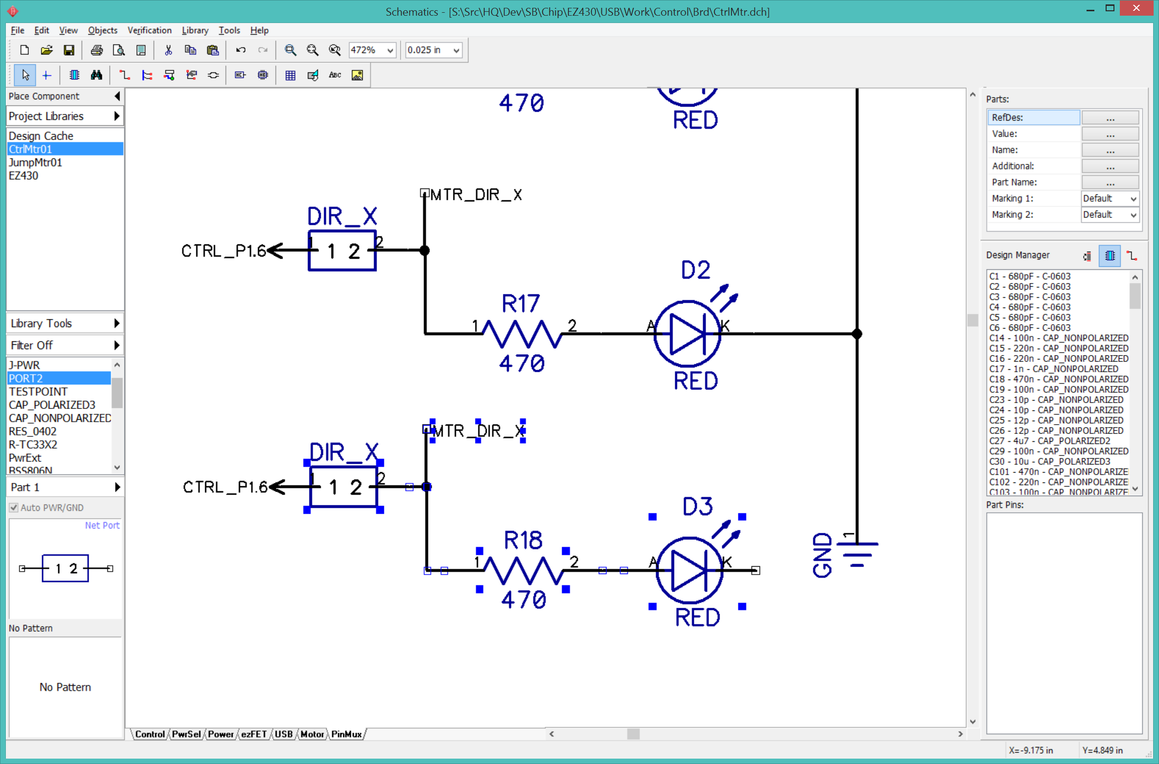
Net Bridge
I want to hang leds from some of the control lines, at least for
the first version. These are frequently the only clue I have available
when debugging the firmware. Rather than cluttering the Control sheet
with leds and resistors, I create a new "PinMux" sheet for the
indicators. The MSP430 side of the wire is named after the MSP430
function and the A3967 side of the wire is named after the A3967 pin.
This provides a natural place to look for the pin mapping, and to
add debug stuff like test points and leds.

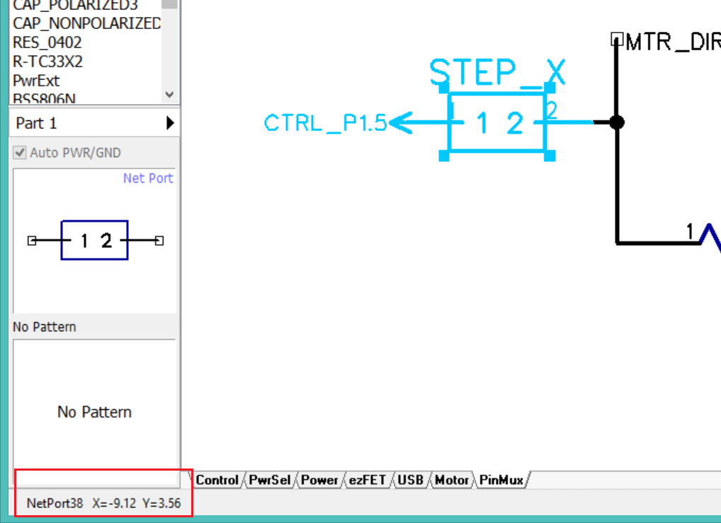
10:15> I ran into a snag with this plan. I don't know how to bridge
two nets without adding a component between them. I need some sort of
phantom component that logically separates the two nets but has no
physical component. This may not be the best solution, but for now I
copied the "PORT2" component from "Components/Net Ports". This is a
2-pin component without any land pattern. I will later create a
pattern that fuses the two pins together, possibly with a test point.
When connecting the ports, right-click the pin and connect it to the
net. This creates a nice external connector symbol that is easier to
recognize than a bare wire.
The 2-pin net port did not do what I expected, although it is
probably doing the right thing. I had somehow assumed the pins of a
net port would gang together multiple nets into the same electrical
connection -- it does not, the pins are not connected. This was not
clear until I was laying out the traces.
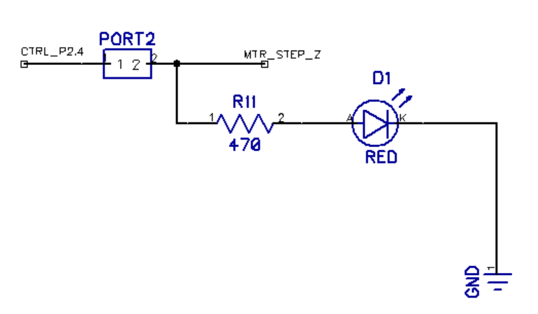
I want the net connected to the MSP to be named "CTRL_3.7" after
the function of the MSP pin, go through a "virtual" pin mux component
and be electrically connected to a different net named "MTR_DIR_Y"
after the A3967 function. All the pin muxes are placed on the same
schematic sheet, making it easy to reassign pins to new functions and
providing a ready cross reference to look up which MSP430 pin is
assigned to what function.
This is not a net port, it is a bridge. The only way to rename a
DipTrace net is to enter a component, so what I want is a "virtual"
component that has two pins that are joined together electrically and
occupies no space.
I created a new component named "BRIDGE2" from TESTPOINT
(Patterns/Misc) and added a second pin, both connected to the same
pad. This generates an error in the pattern editor, but I can ignore
it since it doesn't seem to cause any other problems. This allows me
to create a very compact and informative pinmux sheet.

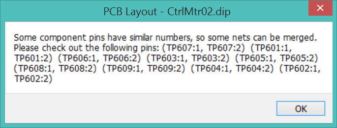
DipTrace Layout gives an informational warning when importing the
schematic, letting me know that the nets sharing the same pin could be
merged in the schematic, and will be merged in the layout.
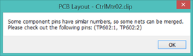
The layout has merged MTR_DIR_Y into CTRL_P3.7, and the MTR_DIR_Y
net is no longer present in the layout although it is still present in
the schematic. The merged net makes all the necessary connection in
the layout. This isn't exactly what I wanted, but it seems to be the
best solution available.
I guess I just need to ignore this warning each time I renew the
layout.

WARNING: I need to double-check the pinmux connections whenever I
touch the associated nets, as DipTrace will see the single pad and
merge the first net onto the second pin of the BRIDGE2 component. This
disconnects the second pin from the second net in the schematic, which
happens without any warning or connectivity errors. This happened when
I added the expansion header and connected the pins to the 5529 pins,
DipTrace silently disconnected all my pinmux BRIDGE2 components. I
fixed this by right-clicking pin2 of each BRIDGE2 component, selecting
"Delete from net", and reconnecting the pin to the second net.
I tried playing more tricks in the component pattern by creating
two pads and then using a manually drawn shapes in the signal layer to
fuse them together. This doesn't work, this triggers DRC errors in
layout.
There is a DipTrace
forum
about a very similar issue, keeping GND and AGND as distinct nets. I
also have this issue, and solved it with a 0-ohm resistor. This is the
officially sanctioned solution, and the only method that doesn't cause
DRC errors. It also has significant problems:
- It introduces a new component that must be placed and routed.
- It uses surface real estate for the 0-ohm resistor.
- It introduces an unnecessary actual part in the BOM.
- It requires placement of unnecessary physical parts during
assembly.
- The bridging must occur on a surface layer, requiring unnecessary
vias.
Each net port needs a unique name; all ports with the same
name will link the same nets. This leads to some very
confusing behavior that will seriously mess up the schematic.
DipTrace has a strange behavior where it remembers which net a
component belonged to even if the wire that joined it is deleted.
Deleting the wire and creating a new wire will rejoin the old net,
which is neither expected nor appreciated. Instead of deleting the
wire, I need to delete the components from the net, which will
implicitly delete the wire, then I can create a new wire with a new
net.
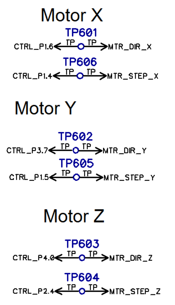
Cloning a PinMux segment is much trickier than it looks. These
are the steps to connect MSP430 pin 26 (P1.5) to A3967 MTR_STEP_Y.
- Create the new net at the source.
Go to the Control sheet, right-click pin 26 on the controller
(MSP430), and select "Add to net...", click "+" to create a new net.
Name the net after the MSP430 pin function, "CTRL_P1.5". Click OK.
This will transform the pin to a net link. I will no longer be able to
connect any wires to the pin.
- Go to the PinMux sheet.
- Select the original sub-circuit and copy/paste to create a new
sub-circuit.
- Rename the PORT component
I need to use a new, unique name. I should not use an existing port
name unless I am sure it is the correct thing to do.
- Remove Net Port pin 1 from the original net.
Right-click pin 1 and select "Disconnect from net". This
will convert the link back to an unconnected pin.
- Add Net Port pin 1 to the new net.
Right-click pin 1 again, select "Add to net...", and select the
newly created net "CTRL_P1.5". This will convert the pin back to
a net link to the MSP430 pin 26 using the "CTRL_P1.5" net.
- Remove Net Port pin 2 from the original net.
Select the Net Port component and note its name, in this case
"NetPort38". Right-click the wire connected to pin 2, select
"Connection Manager...", and delete the two components on either
end of the new wire. In this case, NetPort38 and R18. Click OK.
The wire will be deleted and need to be recreated. Delete the
old net name text, if present.
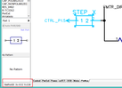
- Add Net Port pin 2 to the destination net.
Draw a wire from net port pin 2 to the second component (R18) and add
a spur that will be used to indicate the connection to the external
A3967 net. Right-click the new wire, select the (old) net name and
rename it to the new destination net name ("MTR_STEP_Y"). Make sure
"Rename Related Wires Only" is checked. Click OK. This should pop up a
confirmation box asking if I want to join an existing net; click Yes.
Right-click the wire again and select "Show Name". The new net name
("MTR_STEP_Y") should be shown.
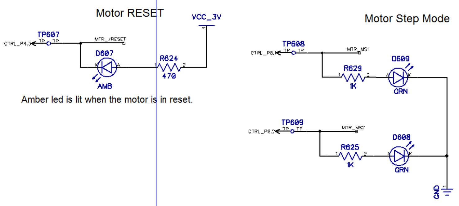
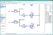
12:20> My finished PinMux sheet. Once I had the technique for
copy/pasting new PinMux blocks it was easy to add an led on every pin
and this design will light up like a Christmas tree. I will probably
delete some of these leds before I start laying it out. I am tempted
to convert the MTR_ connections to "PORT 1" components, but that can
wait until later.
I will add the expansion header to the PinMux sheet. This will be
the bridge between the MSP430 pins and external peripherals such as
limit switches, sensors, indicators, etc.
I still need to add all the parts from the PinMux sheet to the
BOM.
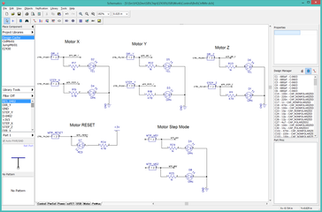
The CtrlMtr schematic design is very nearly complete. Looking at
the PinMux sheet it strikes me that this entire project really boils
down to toggling 3 pins: MTR_STEP_X, _Y, and _Z. Everything else is
just prerequisites.
WebV7 (C)2018 nlited | Rendered by tikope in 114.856ms | 216.73.216.220