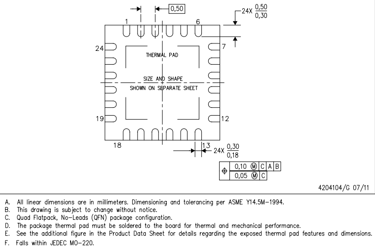
The second step is to create the pattern for the component. The pattern may be copied from a reference library or created from scratch, but it should live in a project-specific library. This step takes longer because it requires extracting the drafting measurements for the pads from the datasheet for the part, which can be frustratingly obtuse. Why can't they just list the co-ordinates and dimensions for every pad in a simple table?
From the drawing, I extract the following:
Create an additional field named "Library" set to the name of the pattern library. This will help later when copying patterns between libraries and projects. Make sure the Pattern Editor is using the correct units, inches or millimeters. Then set the default pad properties (Pattern > Pad Properties) to Surface, Rectangular, Width 0.3, Height 0.5.
IMPORTANT: The origin of the part will be where the Pick-and-Place machine will try to pick up the part. It should be near the center of the part, a location that will provide good suction, and easily identifiable visually when learning the pickup location. It is important that I either have a physical example of the part in hand or at least a photo of the part. This is an touch point between the design and reality.
Pin 1: The PnP machine expects pin 1 to be in the lower left corner and defines this as "Pick angle 0". If the part will always be picked from the tray I am free to put pin 1 in the upper left (where any normal person would expect) so long as I alway put the parts in the tray that way. However, if the parts are to ever be picked up from a tape auto-feeder, I am better off designing the pattern with pin 1 in the lower left corner.
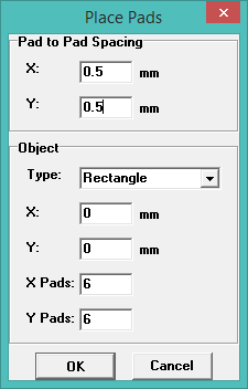 Create a standard square pad layout using Objects > Pads by points:
Pad to Pad Spacing, X=0.5, Y=0.5, Type=Rectangle, X=0.25, Y=0.25, X
pads=6, Y pads=6. (X and Y are offset because it specifies the center
of the pad, and I want the pads to align with the origin.) Add a large
central pad for thermal sink, and some artwork to indicate physical
bounds and orientation.
Create a standard square pad layout using Objects > Pads by points:
Pad to Pad Spacing, X=0.5, Y=0.5, Type=Rectangle, X=0.25, Y=0.25, X
pads=6, Y pads=6. (X and Y are offset because it specifies the center
of the pad, and I want the pads to align with the origin.) Add a large
central pad for thermal sink, and some artwork to indicate physical
bounds and orientation.
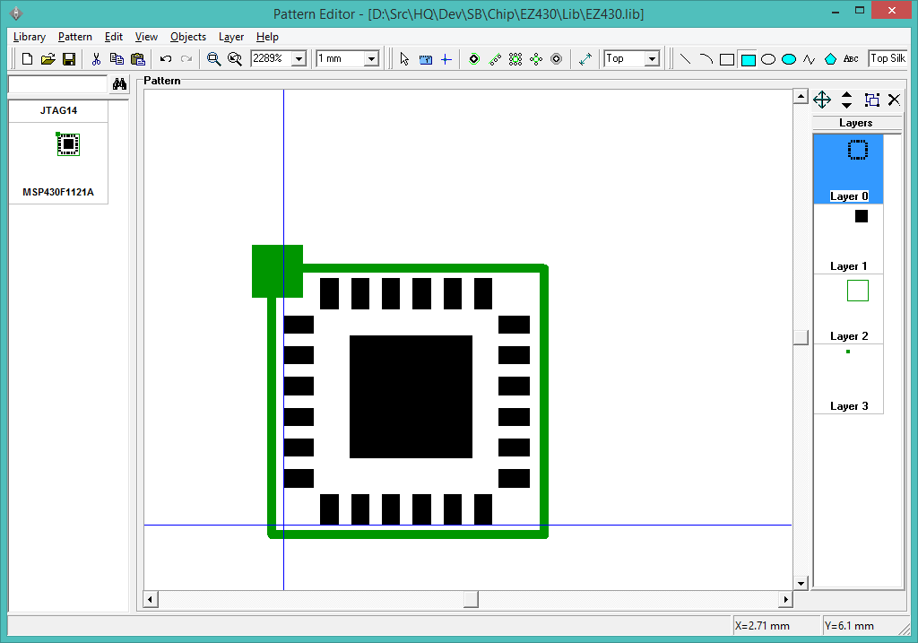
Note that the central pad does not look centered. This makes me think my math has an error somewhere. This will be a minor fix later, so I make a note and move on. [Update: The MSP430 placed perfectly well with a 100% operational percentage, so no fix was required.] I will know later when I print the layout to paper and test fit the actual devices. This is frustrating because the datasheet should just tell me the information, rather than making me (and everyone else) figure it out. Creating the pattern takes longer than the component, but with practice something like the MSP430F1121 shouldn't take more than 30 minutes. It depends mostly on the quality of the information in the datasheet.

Do not place any objects outside the pads. I don't quite understand how, but this seems to create offsets in the PnP locations that cause problems during assembly.
I should avoid putting too much silkscreen text in the pattern because I don't know yet how this text will be oriented on the board. The exception is to mark clearances or keep-out areas; these should be part of the pattern. If I update the pattern after it has already been included into the schematic, I will need to "Replace Pattern" (with the same pattern) to update. (Also, I need to click on the library name to reload its contents.)
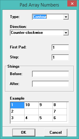
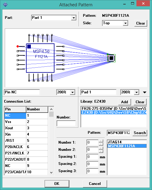
Save the updated pattern library, reopen the component library, select the MSP430, and attach the pattern to the component using Component > Attached Pattern ... If the pattern library is not already listed in the Library listbox, click Add and navigate to it. Select the library, then select the pattern. (I may need to reclick the library to refresh the contents.) DipTrace will connect component pin 1 to pattern pad 1 and illustrate the connections. Verify that the connections are correct by mousing over the pins or walking through the connection list.
Save the updated component library.
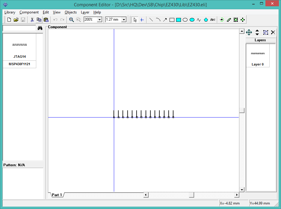
This is a much easier component, and take only 15 minutes to create both the component and pattern. The component is simply a row of 14 pins, with names from the table above.
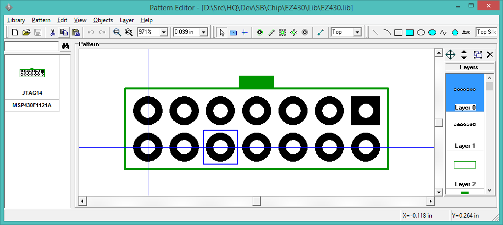
The pattern is two rows of standard 0.1" header holes (round through-hole, width 0.08", hole diameter 0.04".
This component took all of about 10 minutes to create.