2014-07-21 19:39:12 chip
Page 1062
📢 PUBLIC
I am starting from scratch, so I will be creating all the
components as well as the schematic. The first data entry step is to
create the component library for the project, starting with the two
components I know: MSP430F1121A and the JTAG connector. I am sure
there will be others, but the first components I want to drop into the
schematic are these, so there is no point to opening the schematic
editor until I have them.
Every project needs its own component and pattern libraries. The
internal name (not file name) of the component library should be
"Project Components" and the internal name of the pattern
library should be "Project Patterns". The "component" and
"pattern" suffixes are important when I add both the component and
pattern libraries to the layout project and DipTrace lists both
names.
Creating new components is a two-step process, first create the
component in the Component editor. Every component lives in a library,
there is no option (other than exporting as an ascii file) to save an
individual component. It is easy to have many libraries scattered
around in many projects. However, all components in the project
should be in the project-specific library. Even the basic
resistors, caps, etc should be copied from the standard library into
the project library. This protects the project from changes to the
reference library that may happen later. Once the project is complete
the new and updated components and patterns should be copied (back)
into the master library.
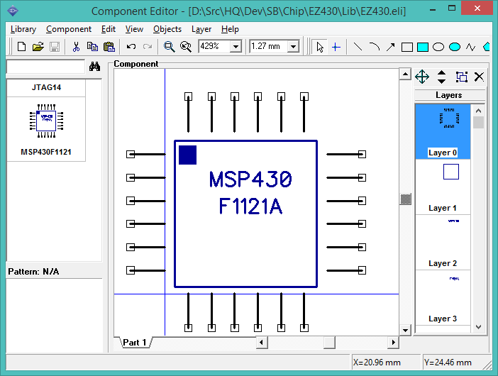
In the component editor, create a pin for every connection point on
the component. The location and orientation do not matter, as this is
just for the schematic. Add shapes to make the component recognizable
on the schematic, but it does not need to have any relation to its
physical appearance. Name the pins, but make sure the pin names
match the pin number on the physical part. This is critical, as it
is how the schematic pins will be mapped to the board layout pads
later.
Each pin can be assigned "Type" and "Electric" properties. It
would be nice if these properties
were used to assign the net classes in the layout, but that doesn't
seem to be possible. It seems these properties are only used for
Spice analysis.
Create an additional field for the component named "Library" and
set it to the component library name. Create a field named "PnP" and
set it to "SMT", "Hand", or "None". Add as many additional fields as
needed, more information is always better than less (provided it is
correct!).
It is my experience that creating a new component is a very short
and quick task. So short that except for very large IC's with many
pins, it is quicker to create a new component from scratch than to
hunt for a component created by someone else. In addition, it is
critical to use a naming scheme that is consistent with the PnP
parts library. See . Creating the component for the
MSP430F1121A with 24 pins takes about 10 minutes.

If there is an existing component in another library, I can copy
the component by first creating a new blank component in my
current library and then importing from the other library using
"Component > Get from library...". Make sure to set the Library
field to the name of this (destination) library.
Using the default settings, the size of the passive components
(resistors, caps, etc) is out of scale (too large) compared to the
multi-pin IC components. The scale is better if the spacing between
the pins is increased from 2.54mm (1/10") to 5mm (1/5").
WebV7 (C)2018 nlited | Rendered by tikope in 91.500ms | 216.73.216.220