May 23 2016
Today's task: Create a new paste stencil from the 20160511 layout. Tweaking the paste apertures in the layout is not the preferred method, but it lets me continue to use the remaining 3 boards.
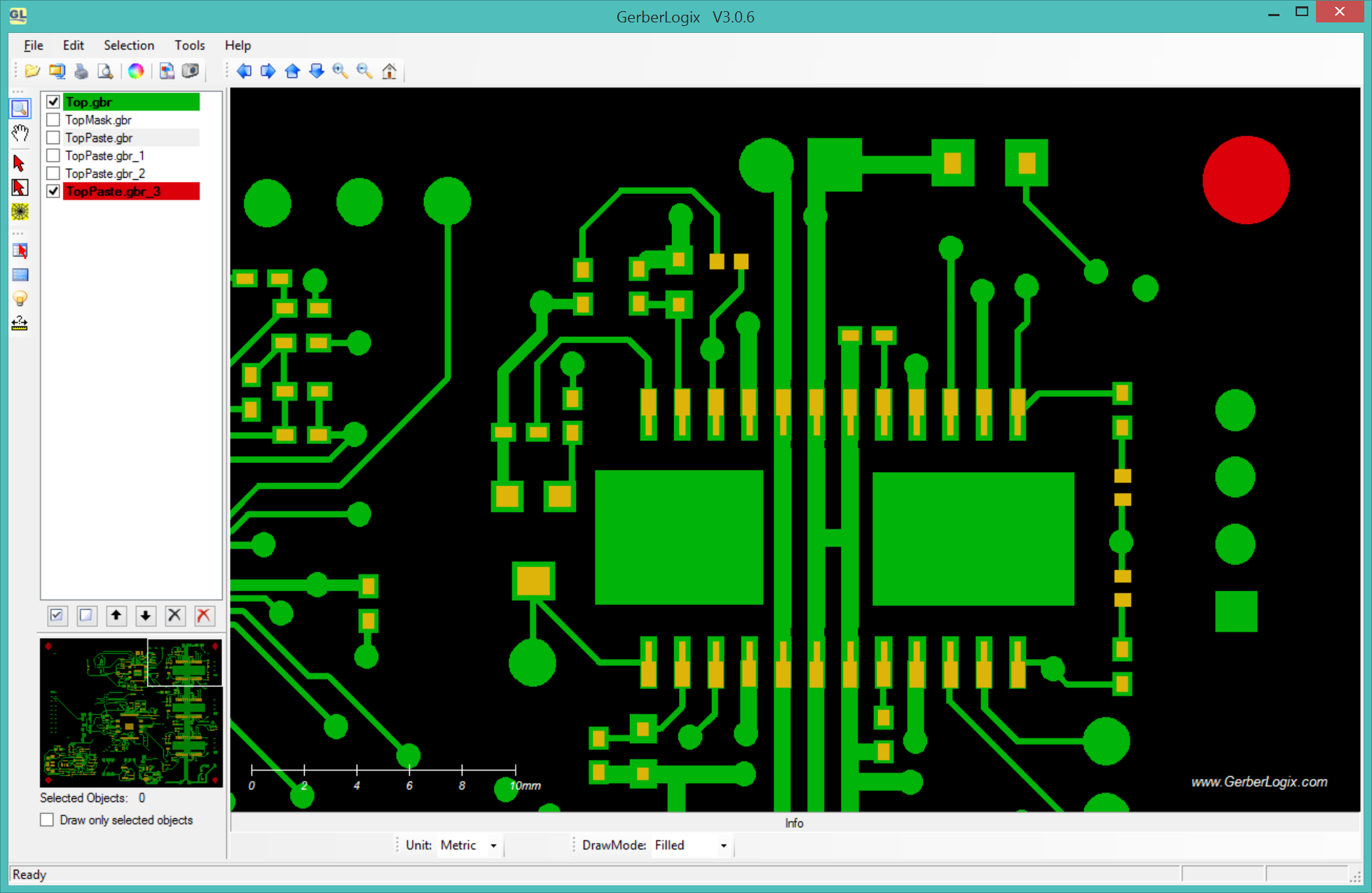
I copied the DipTrace files from the 20160511 archive to a new folder "20160523" and launched Layout. I am tweaking the pads directly in the layout, so this should not change the component libraries or schematic. This is a tedious process of selecting a pad in the layout and setting the paste shrink value. I don't need to select every pad, I can set the shrink for all similar pads. Then I need to very carefully review the results in the Gerber files.
Make sure the units are set to millimeters!
I select the component and check the properties. If it a standard 0402, 0603, or 1206 component I use the shrink value from the table (). If it is a pad for an IC with 0.5mm pitch, I use 0.05mm. Other pads as judgement calls.
The "Pads of selected patterns" does not apply to unselected components that use the same pattern as the selected component. Using the "Similar pads" option seems safe, I want to apply the paste shrink regardless the actual component.
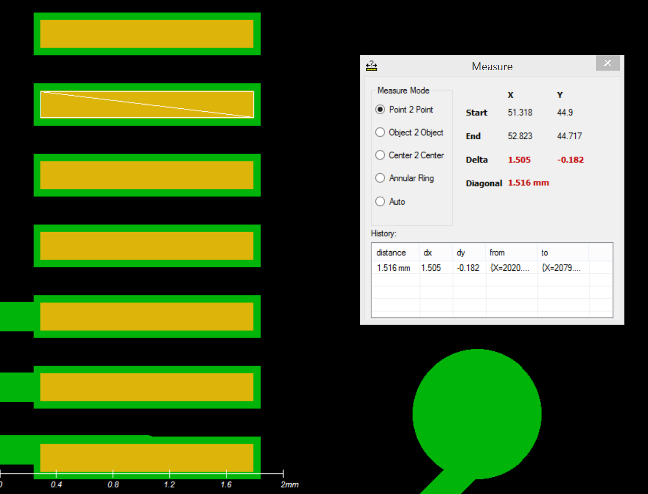
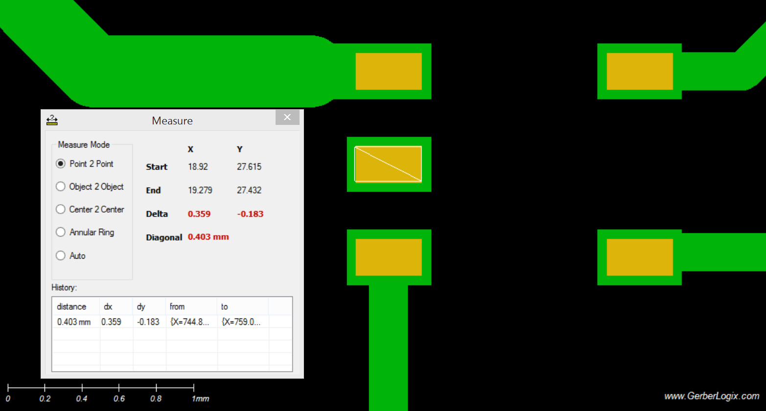
The smallest component is the 0402 led. A paste shrink of 0.15mm results in two paste areas of 0.30x0.20mm, very near the limits of the stencil. My concern now is that the paste area may be too small to catch both ends, resulting in bounced or tombstoned parts.
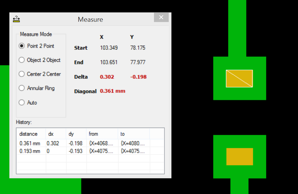
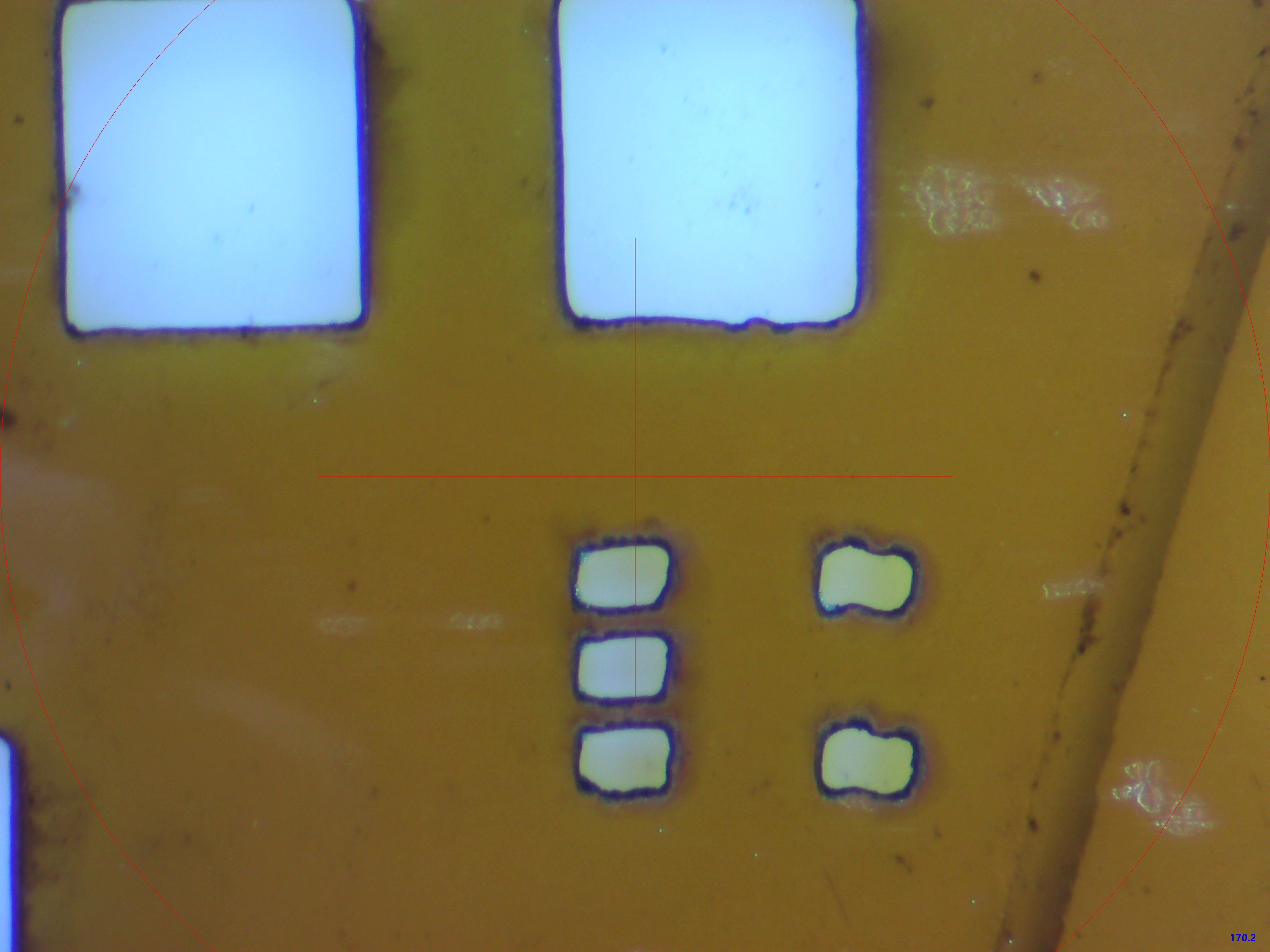
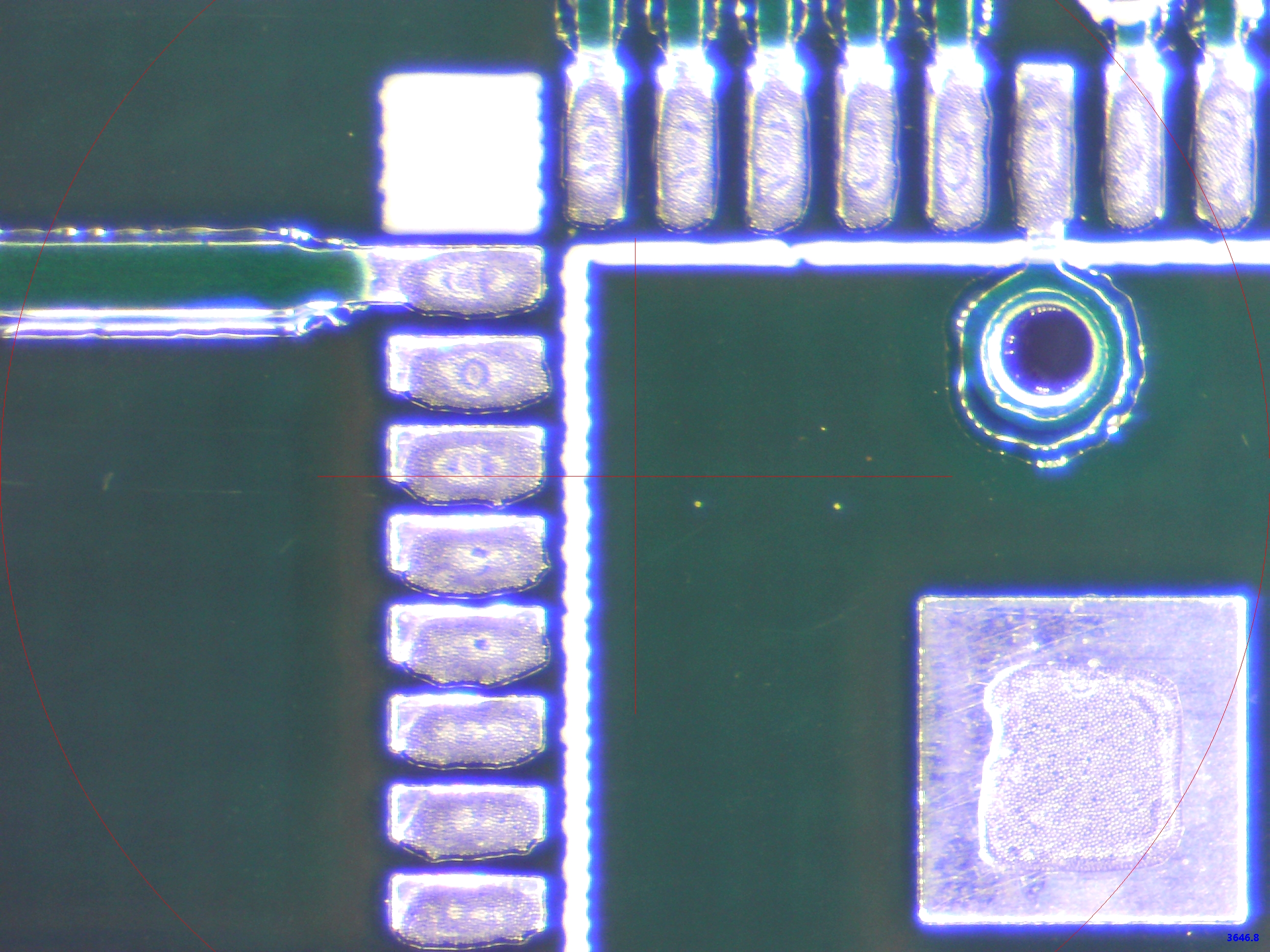
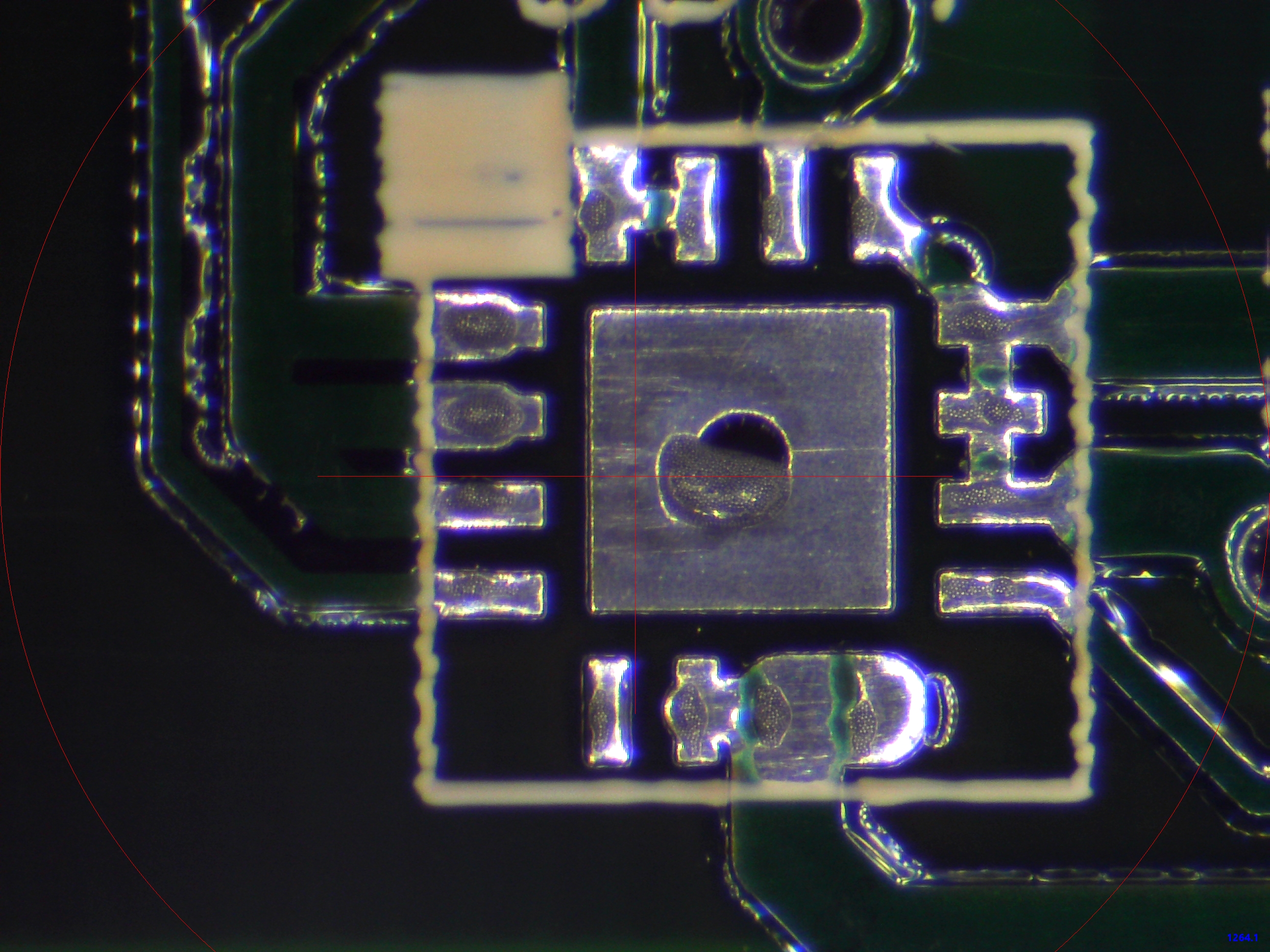
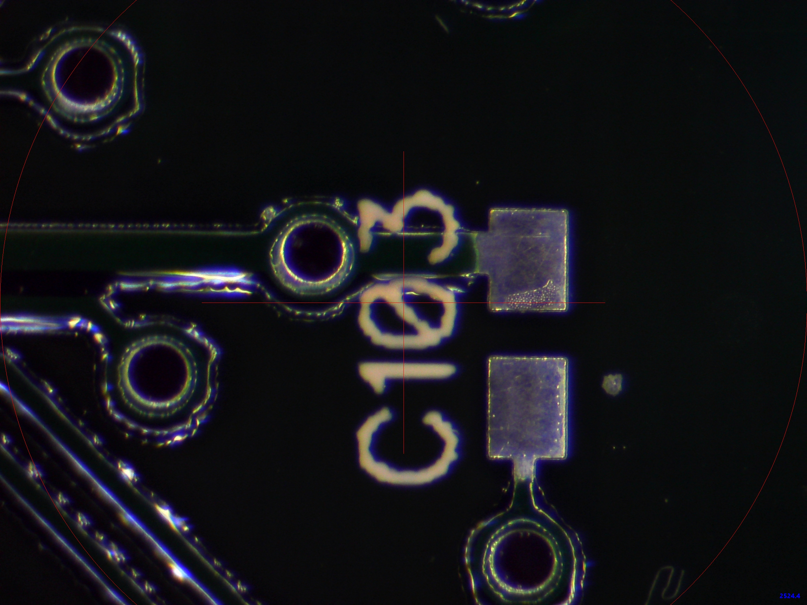
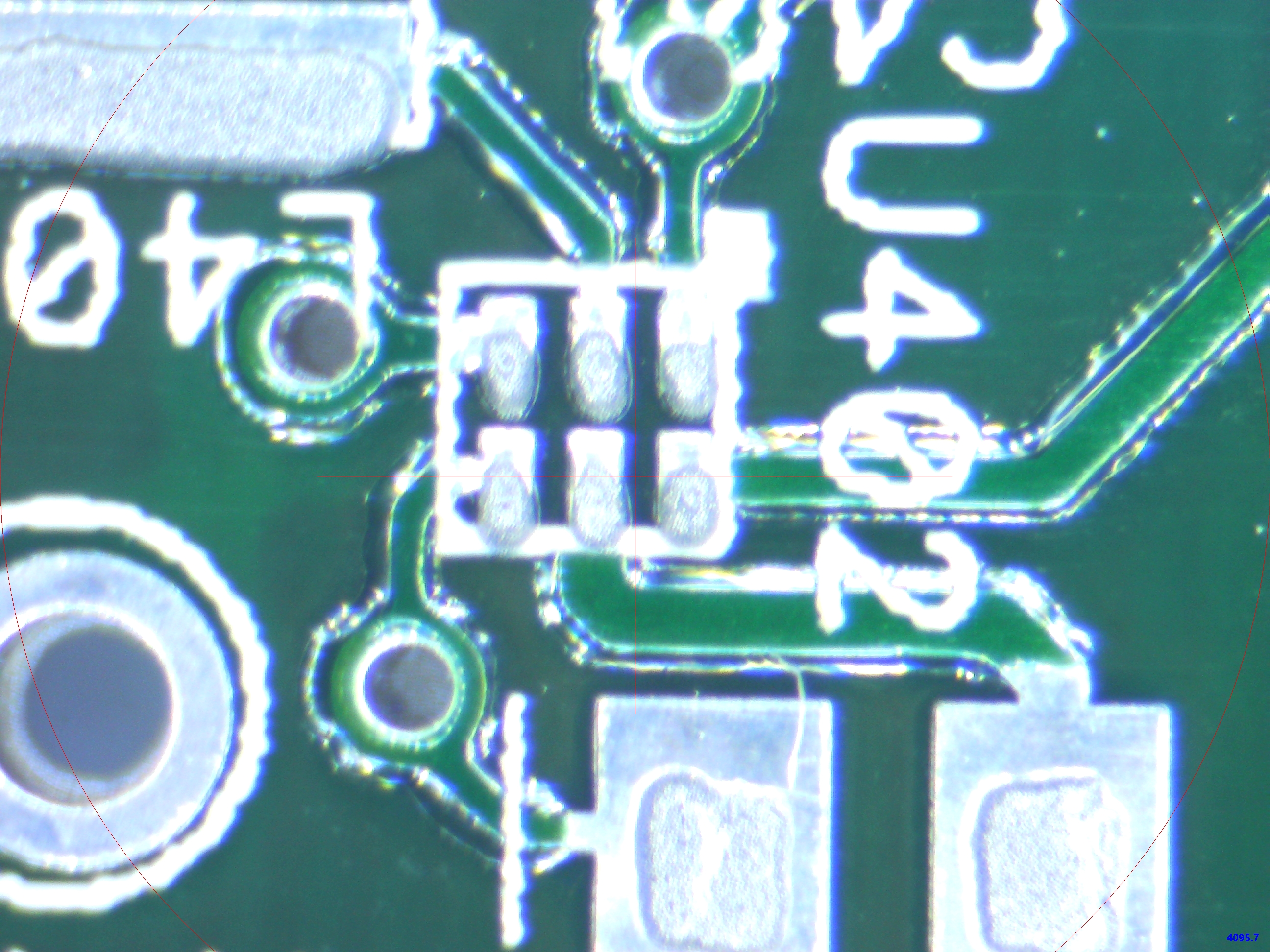
The pads for the 5529 are 1.5x0.18mm. I expect these to result in slits about 0.20mm wide.
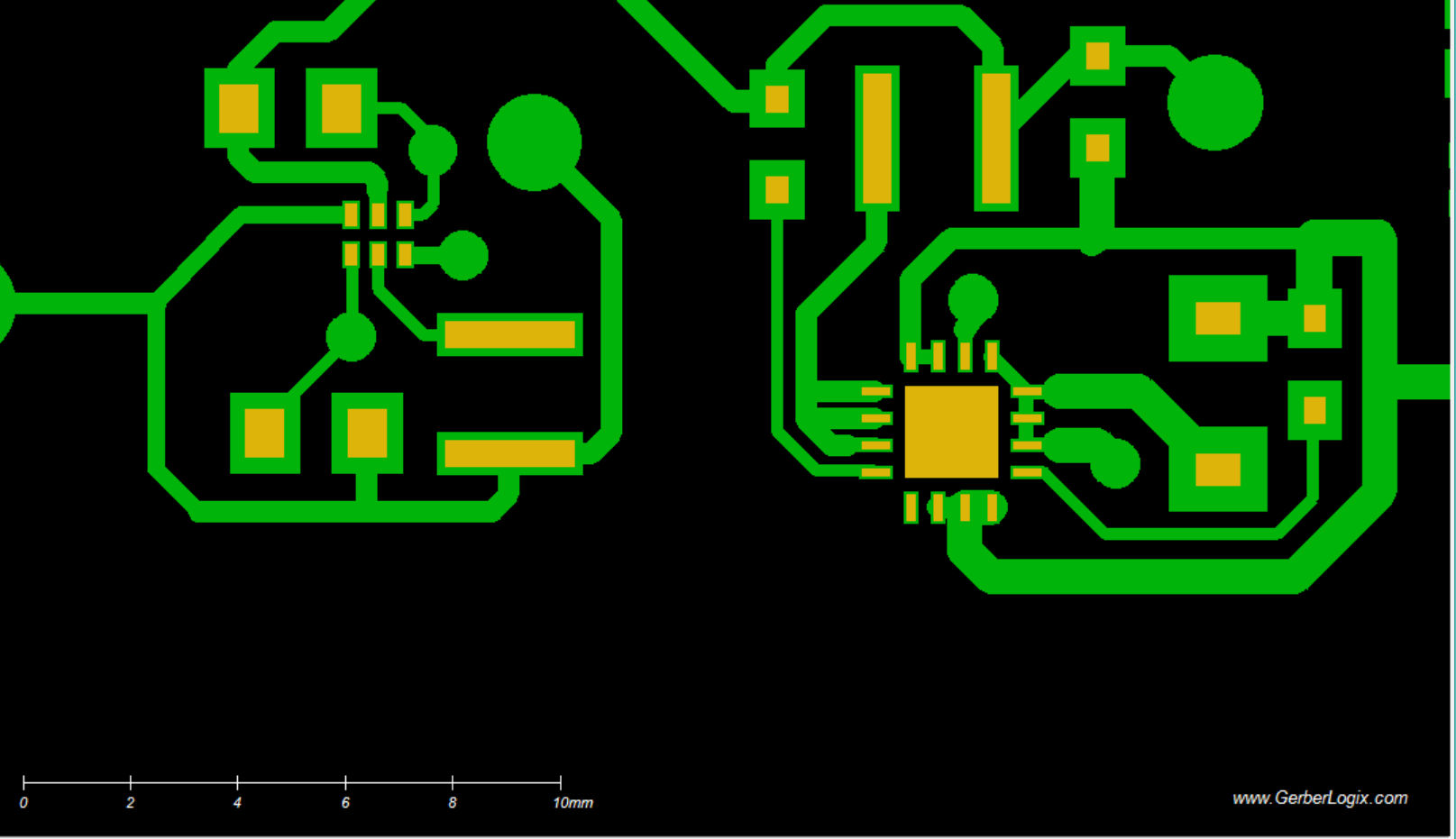
The two tiny power ICs look much better now.
The TPD2E pads are 0.36x0.18mm.
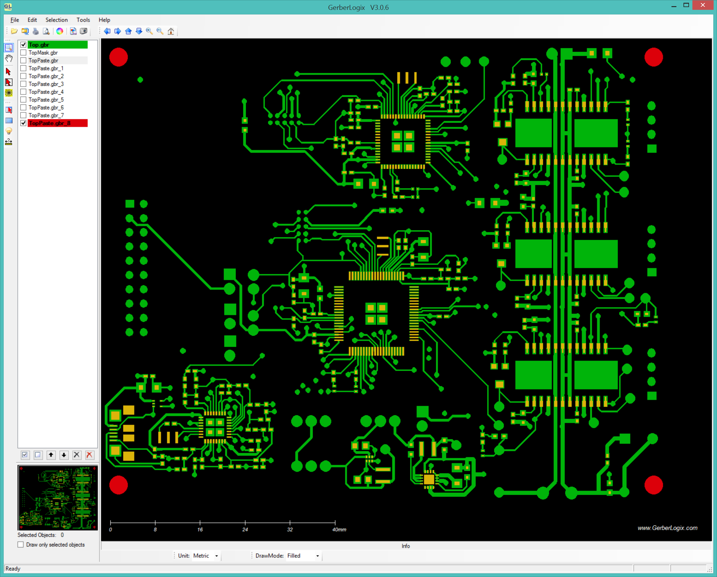
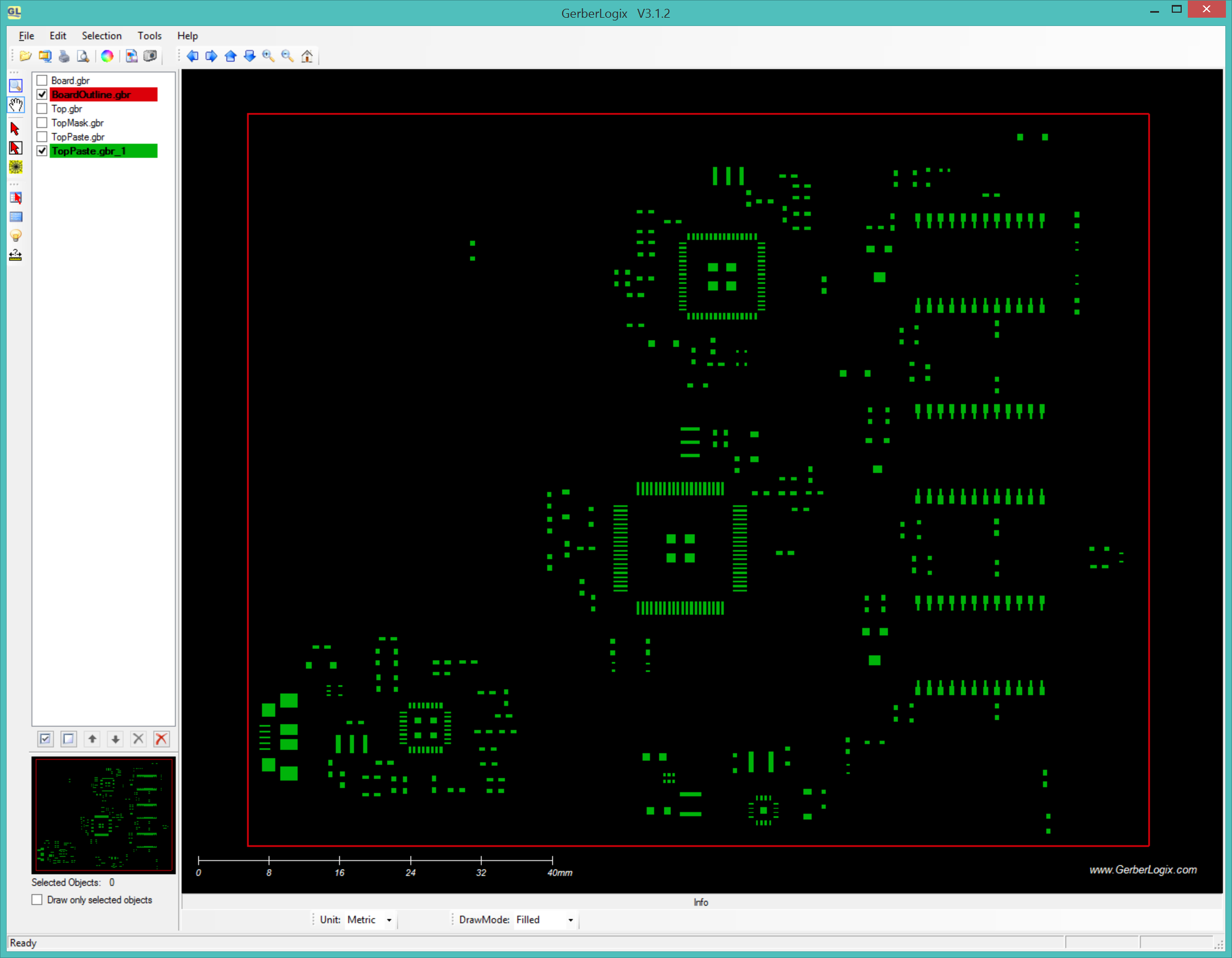
The gerber viewer was a tremendous help for this task. The high contrast colors made it very easy to find the pads that needed to be tweaked. The entire process took about 45 minutes, much quicker than I expected.
Don't forget to delete the mounting holes from the stencil gerber!
I post this to OHaraRP.com (Order 2888) and wait to see how the tiny apertures turn out.
Now I need to revisit the CtrlMtr and CANMtr projects to update the component libraries with the proper paste shrink modifiers. Hopefully, this will prevent similar problems in the future.
May 25 2016
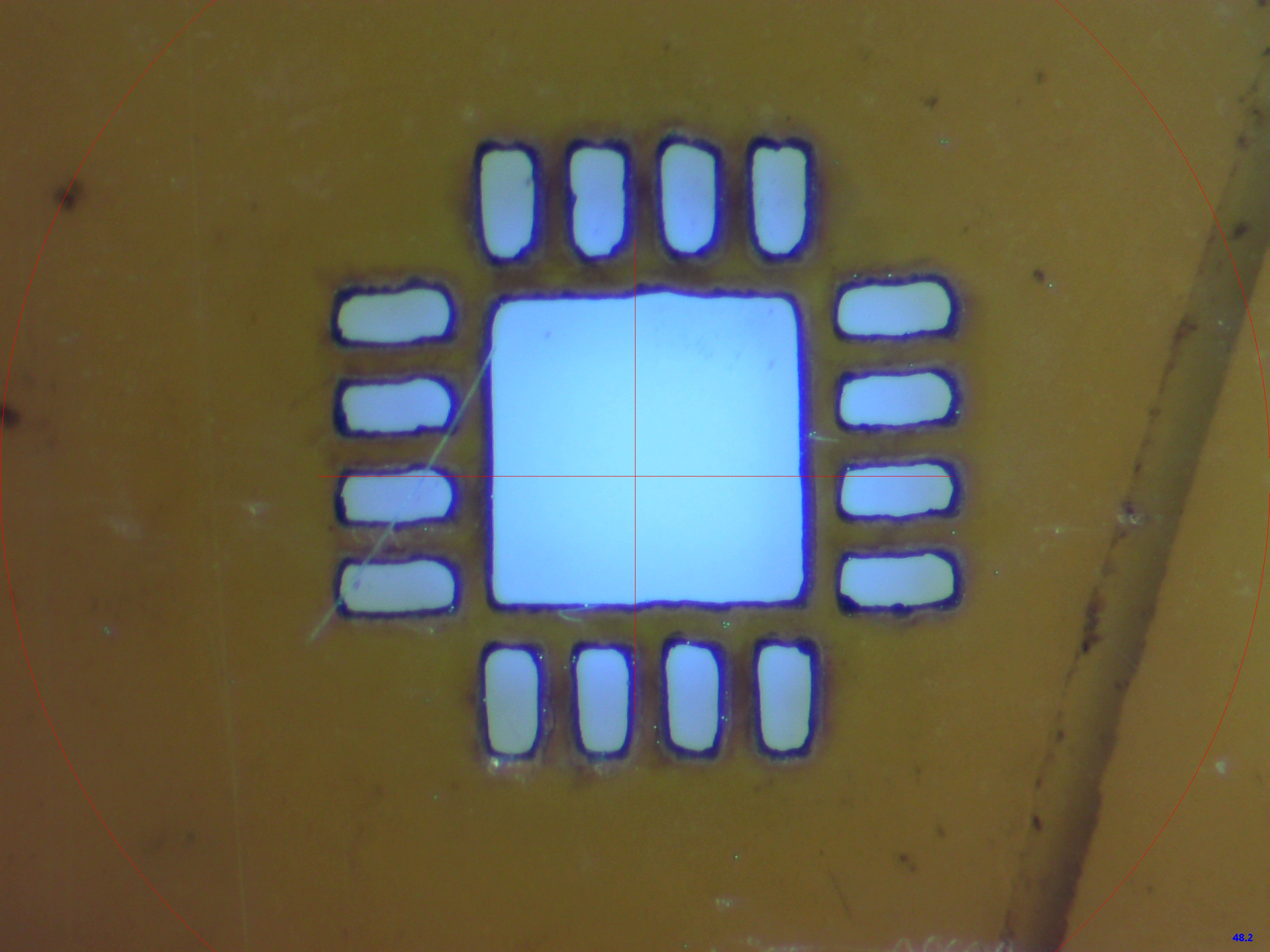
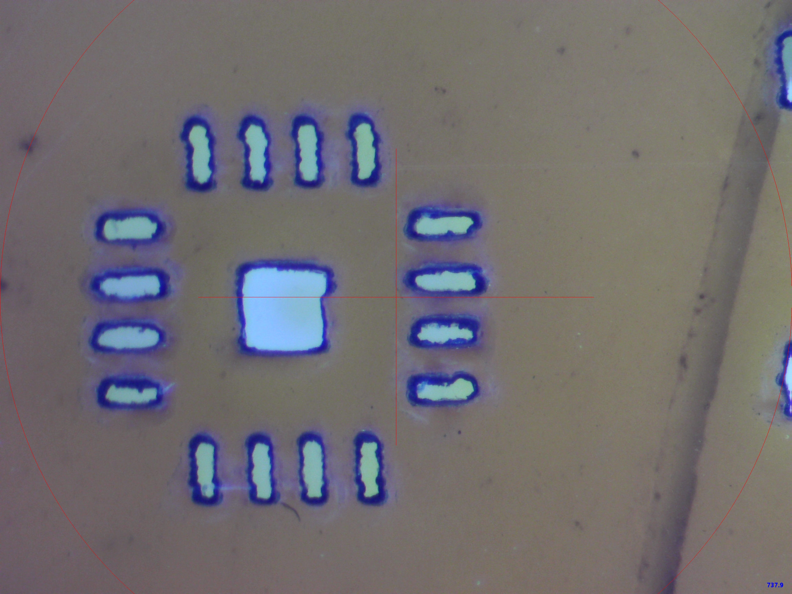
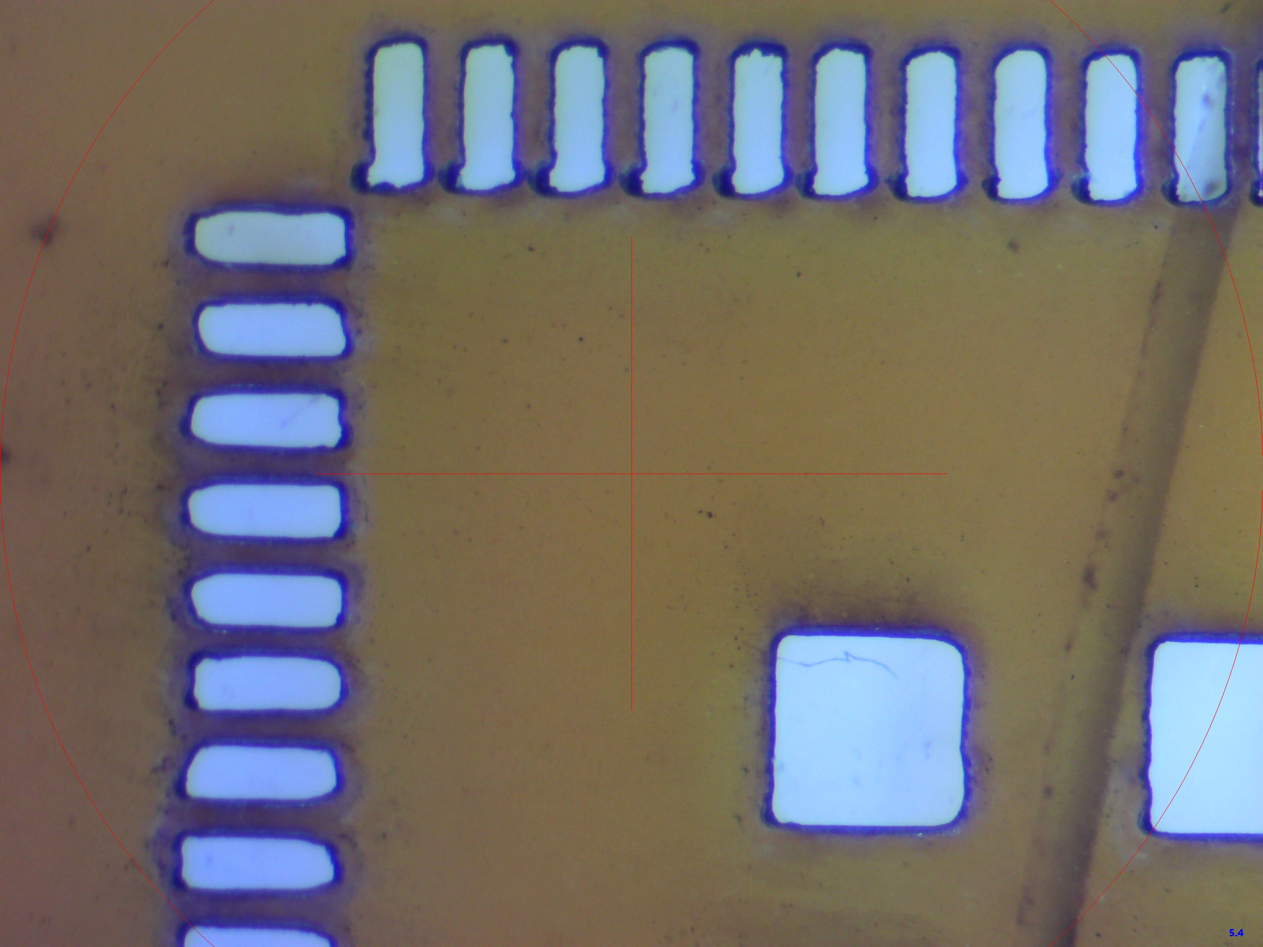
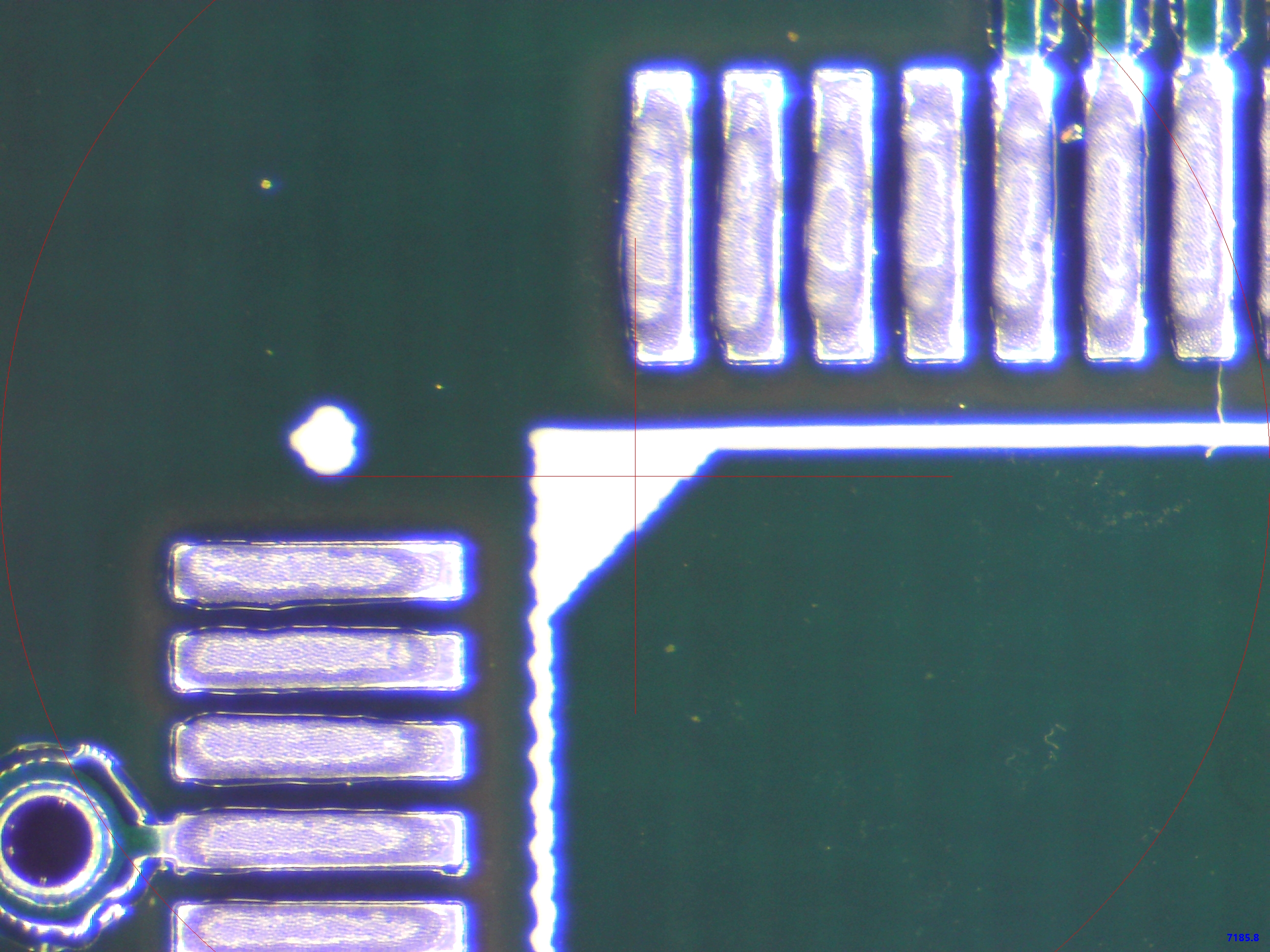
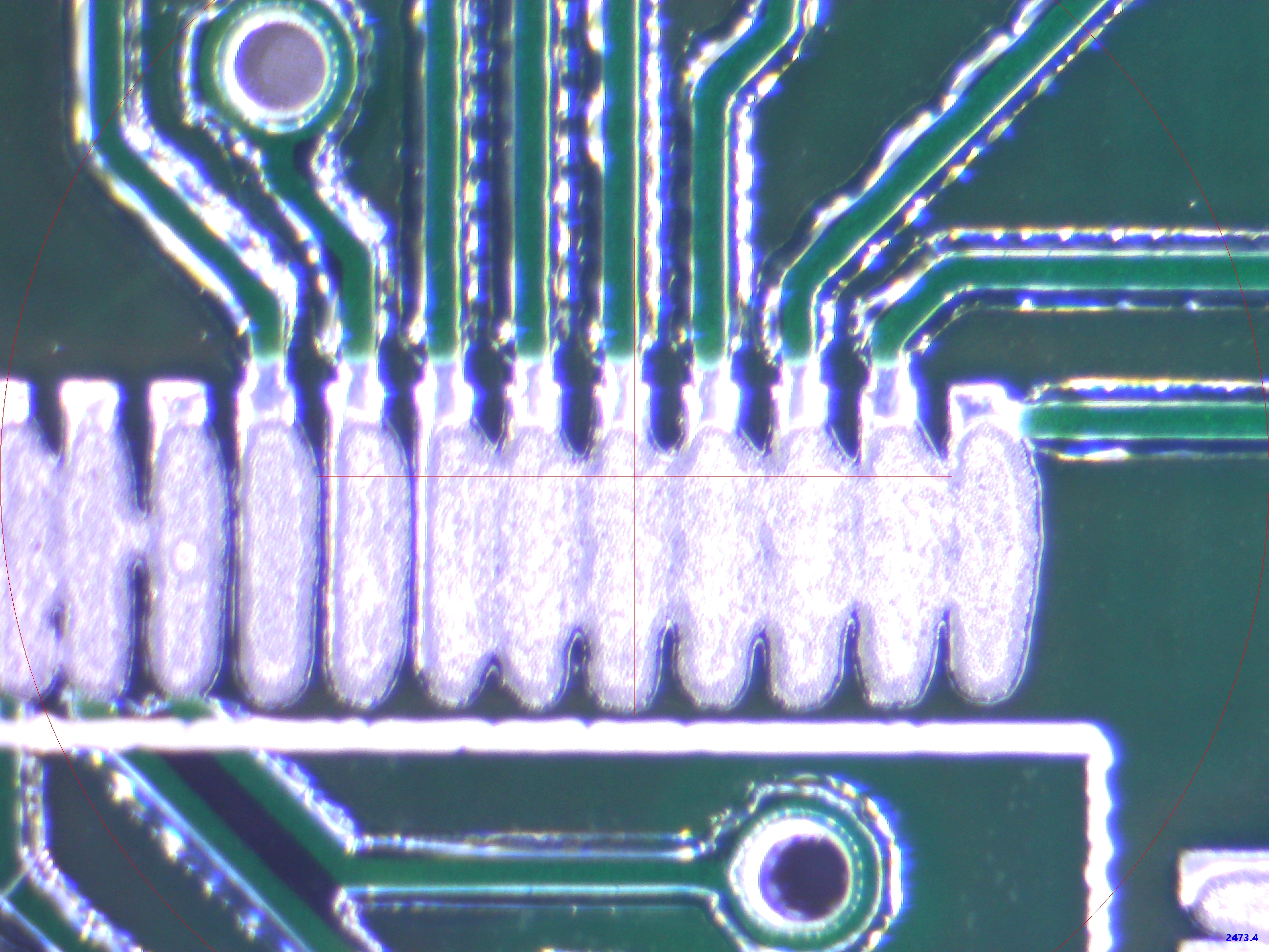
1335> The stencil and resupply parts arrived today. The new stencil looks better. The tiny pads for the TPD2E are just dots, which was expected. This is almost the smallest hole the laser can make. I am not too concerned about the ragged shape of the holes, the stencil serves more as a sieve to control the amount of solder on the pad; it doesn't need to square the corners.
Without Paste Shrink
With Paste Shrink
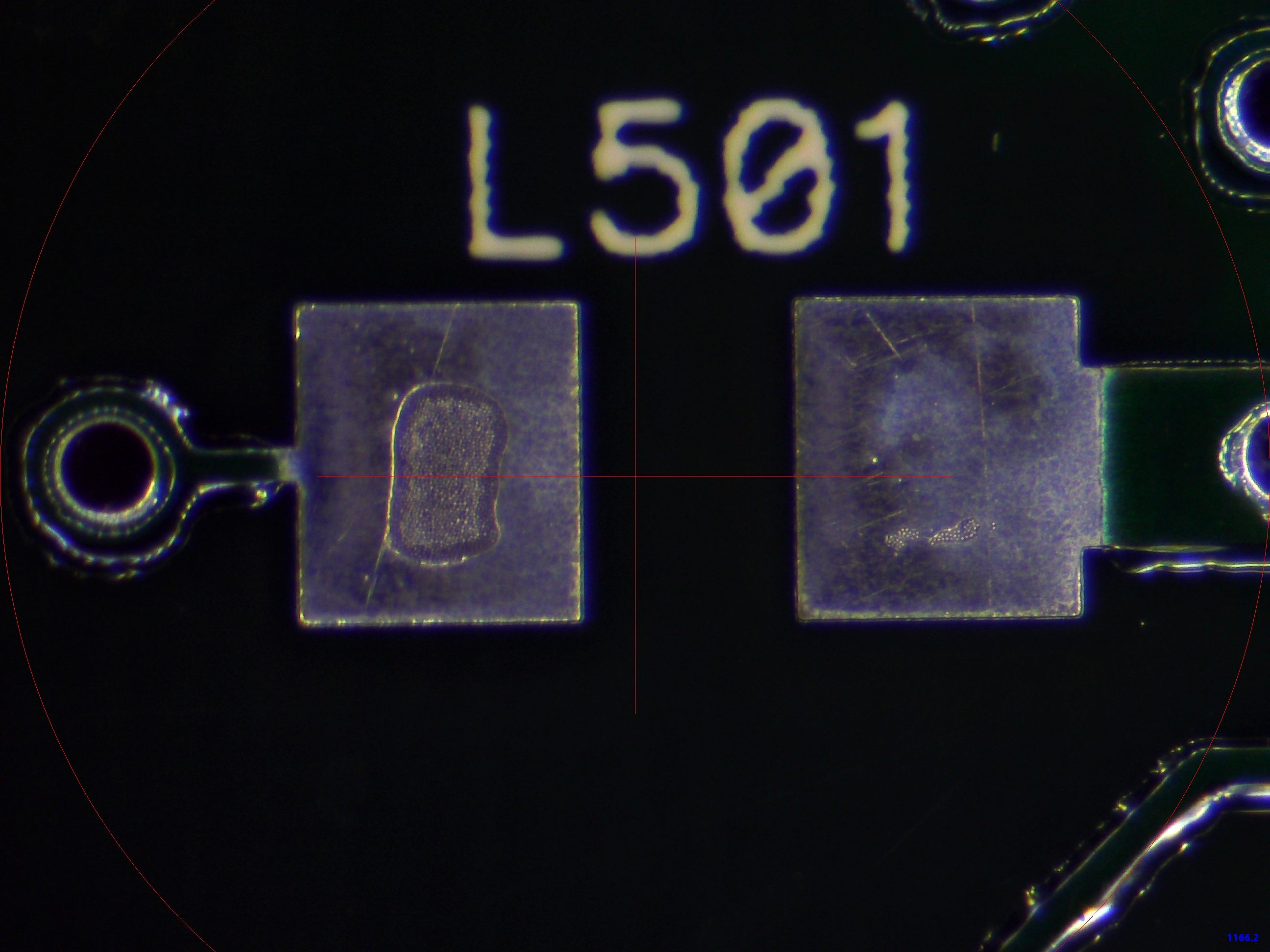
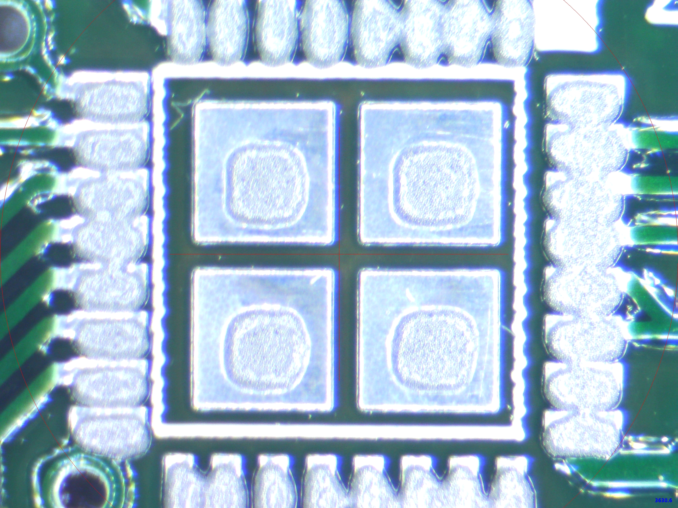
I am concerned I didn't shrink the MSP430 pads enough...
The machine is already loaded and ready to go. The goal is to run a build and see if I can talk to the two MSP430s, so I am leaving the replacement yellow leds in place for now. The solder paste is warming up.
1348> I am restocking the tray.
1447> Tray is loaded and programmed, autofeeders have been checked.
1447> Applying solder paste.
1610> After a few placement problems, the board is complete and is now in the oven.
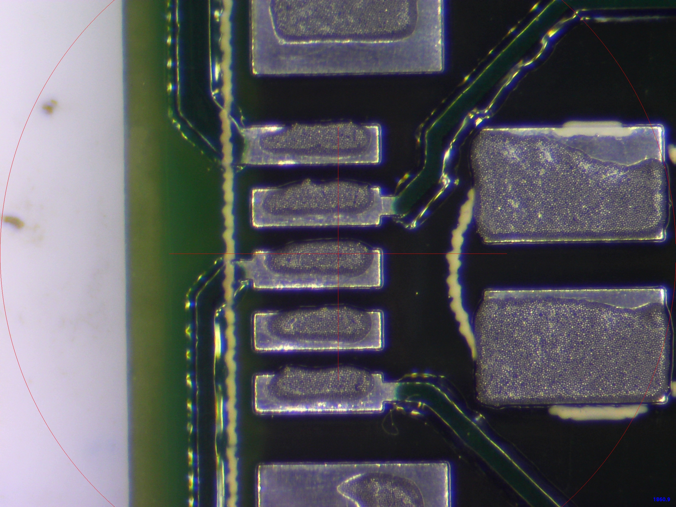
I ran the vision inspection after the build. This build looks better than the previous, but there are still problems and my expectations are low. There is still far too much solder on the fine-pitched ICs. I need to shrink the pads down to just slits, especially when there are 80 of them. The paste dots on the 0402 pads are too small, failing to catch both ends of many parts. I expect to have multiple tombstones when the board comes out of the oven. The 0402 paste apertures need to be made a bit larger -- perhaps a shrink of 0.10. Even better, I could offset the paste apertures closer to the center, but this means creating custom paste shapes in the component library. But only for 2 components: R0402 and C0402.
Components that have been put down into paste cannot be reused unless I take extreme care to remove all traces of solder. Even a tiny speck of solder is enough to make the vision system reject the part. Old solder can also make the part stick to its tape compartment and fail to pick properly. This caused the build to fail on 4 components.
1624> The board is out of the oven.
It is clear that for the very small or finely-pitched components, paste shrink alone is not enough to guarantee goods results. I will need to create custom paste apertures in the component patterns.
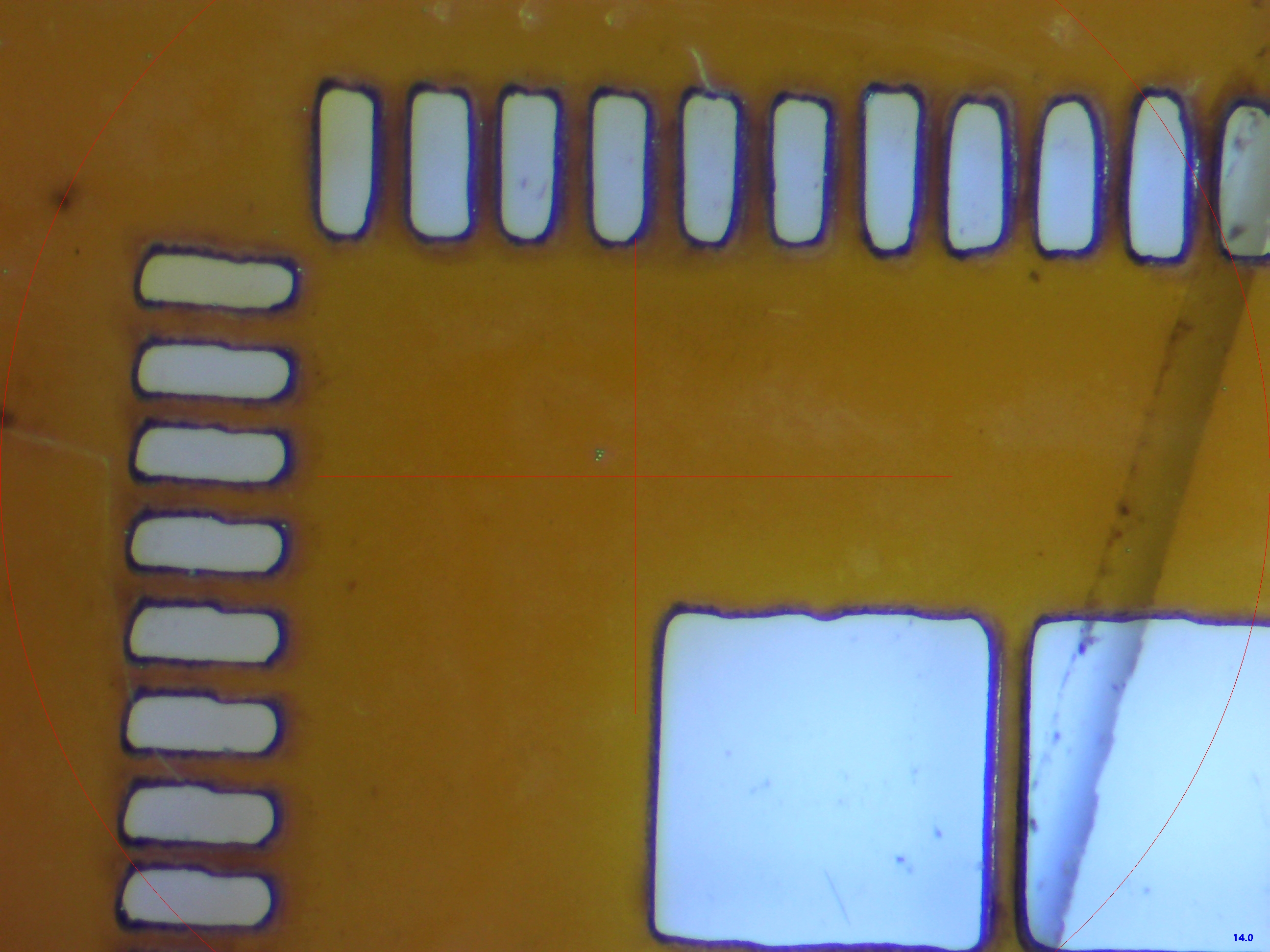
I will be testing the lower limits of the resolution of stencil features. The smallest feature so far has been the TPD2E with pads 0.40x0.35mm, which were a bit ragged but OK. I am assuming the beam width is between 0.15mm and 0.20mm and the resolution is 0.01mm.
There are three criteria for the paste apertures:
The worst-case scenarios:
The 0402 pieces failed because the solder dots were too far apart to catch a slightly (on the order of tens of microns) misplaced part. The amount of solder was correct, it was just enough to fill the pad, and I do not want to increase the solder area by simply reducing the paste shrink value. The paste needs to be moved and reshaped so that it will always catch the ends of the part with the same amount of paste. This requires a custom paste aperture. Fortunately, there are only four patterns that are used by all the 0402's: R0402, C0402, C0402+, and D0402 and they will all use the same apertures.
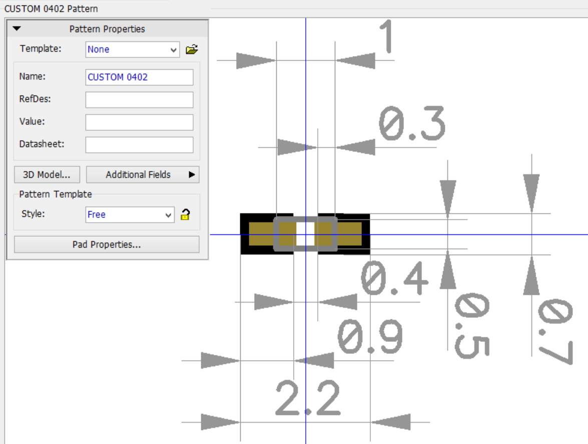
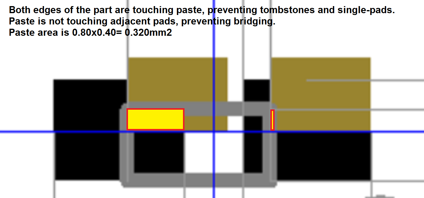
The pads were 0.90x0.70mm with a paste shrink of 0.15 for a paste area of 0.75x0.55= 0.4125mm2. Keeping the area of the paste under 0.50mm2, I want to put a strip across the width of the pad near the center edge.
Covering the worst-case misalignment of both stencil and part required extending the paste 0.05mm beyond the inner edge of the pad. I believe the Wicking Gods will pull the paste onto the pad during reflow. The overrun cannot be covered by extending the edge of the pad, this would create a bridge in the worst case.
Part: (-0.6,-0.25),(0.5,0.25)
Paste1: (-0.95,-0.20),(-0.15,0.20)
Paste2: (0.15,-0.20),(0.95,0.20) = 0.80x0.40= 0.320mm2
This makes the aspect ratio of the paste wider and shorter compared
to the pad.
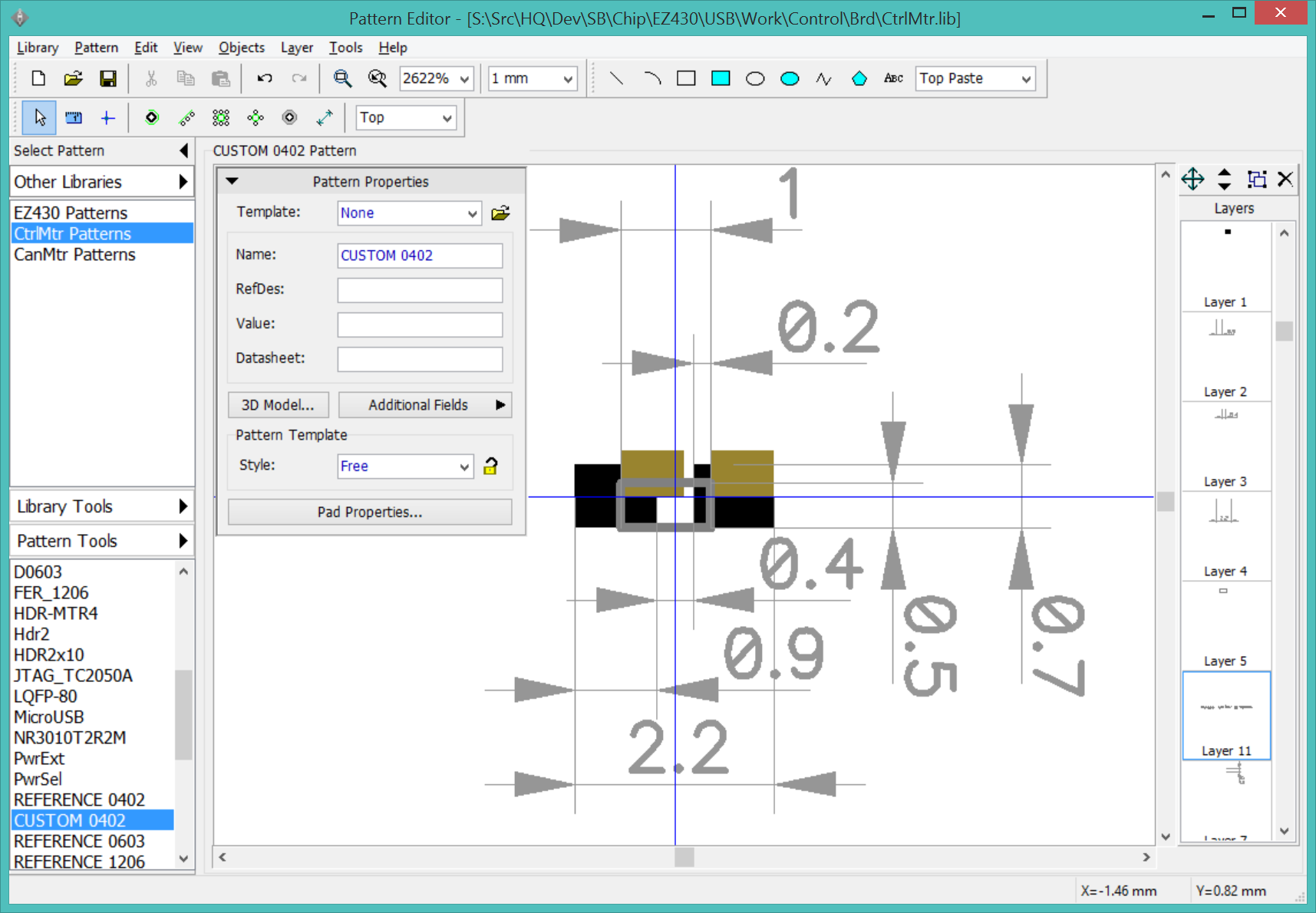
Disable paste, manually create paste shapes 0.14x1.0mm, corners offsets from the center of the pad: (-0.07,-0.70),(+0.07,+0.30)
I was working on the MSPs when I had a nagging thought: I was able to build board with 0.5mm pads before, without resorting to custom paste. I began to wonder if the problem was in applying the paste, not the stencil. Did I simply mess it up? This would be very good news, because I could test this theory without spending any more time or waiting for deliveries. I just needed to take even more extreme care aligning the stencil, and thoroughly wash the stencil and board each time.
The results were very encouraging! I think this board would have worked.
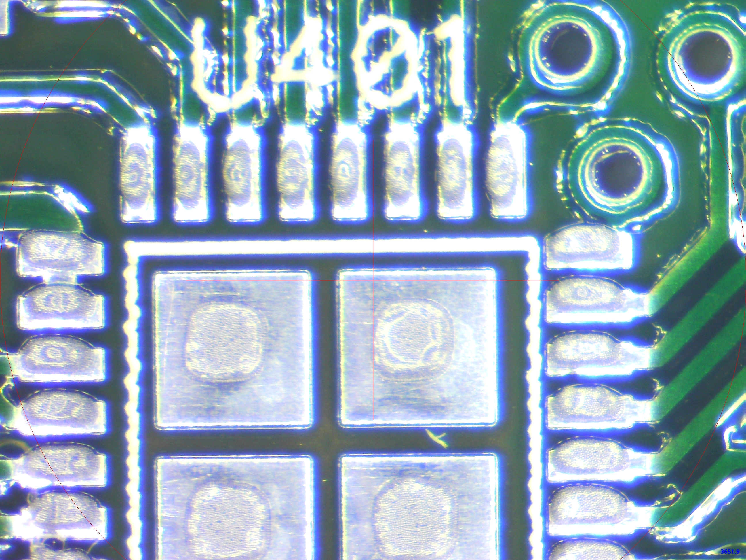
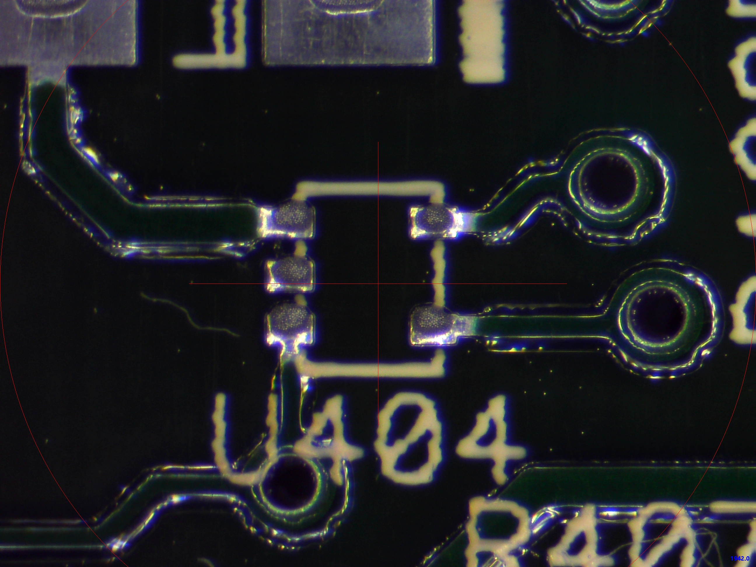
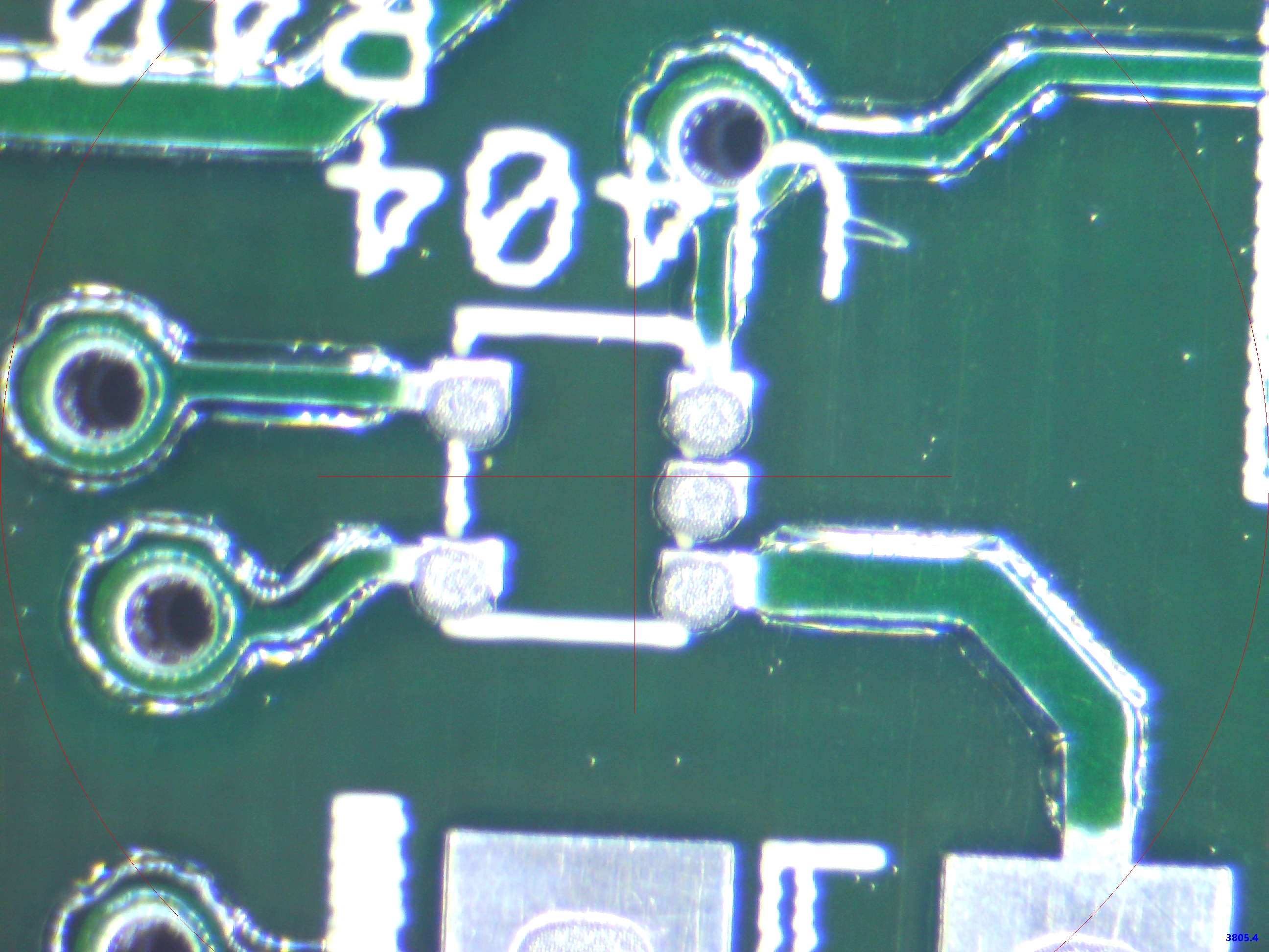
NOTE: Pins 1 and 2 of the USB hub (U401) are tied together, I would expect these pads to fuse together. This is another reason why the traces should be joined well away from the pad; do not run traces directly between two pads.
The only significant problems:
I learned some things:
So the ideal application is 3 passes:
I am making another run at a board...
1542> Restocking the tray.
1616> Tray is reloaded, now learning tray pick.
1643> Tray pick learned. now check place list.
1645> Place checked, now aligning stencil.
1652> Stencil aligned, looks good under the scope. It is very easy to be fooled by parallax! Trust that if both the MSP430s are aligned, the rest of the board must be also unless I have ripped or wrinkled the stencil.
1702> Paste complete. QA check failed on both MSPs, U401 (hub).
On the bright side, TPD2E, U402 (power regulator), U301 (power converter), and everything else look good. The only problem was too much solder on the MSPs. And probably the microUSB, but that can be fixed by a delicate pre-assembly operation.
The paste alignment was perfect, zero missed pads. I seem to have learned that skill today. Now I need to work on my squeegee technique. Sooooo close, but still a reject.
May 28 2016
I am forging ahead with Stencil #2, I was making real progress yesterday and I feel I can make it work.
Scraping the solder slowly, and with firm pressure seems to work best. The large MSPs need to be scraped diagonally. I take my time and use 4 strokes: only once across the MSPs, across the A3967s, down along the power and USB blocks, and the last stroke to touch up any missed pads.
1230> I may have a winner... the paste looks as good as I could possibly expect, with no touching pads on the MSP430s (or anywhere else) and no missing pads. I am moving forward with placement.
1300> Still looking good... The placement completed with 2 bad picks (one was operator error, forgot to remove the cover tape) and 2 bad places. I reran the bad places easily. The tray was fixed and the bad picks completed. Visual inspection still looks good, and I am moving forward to the oven.
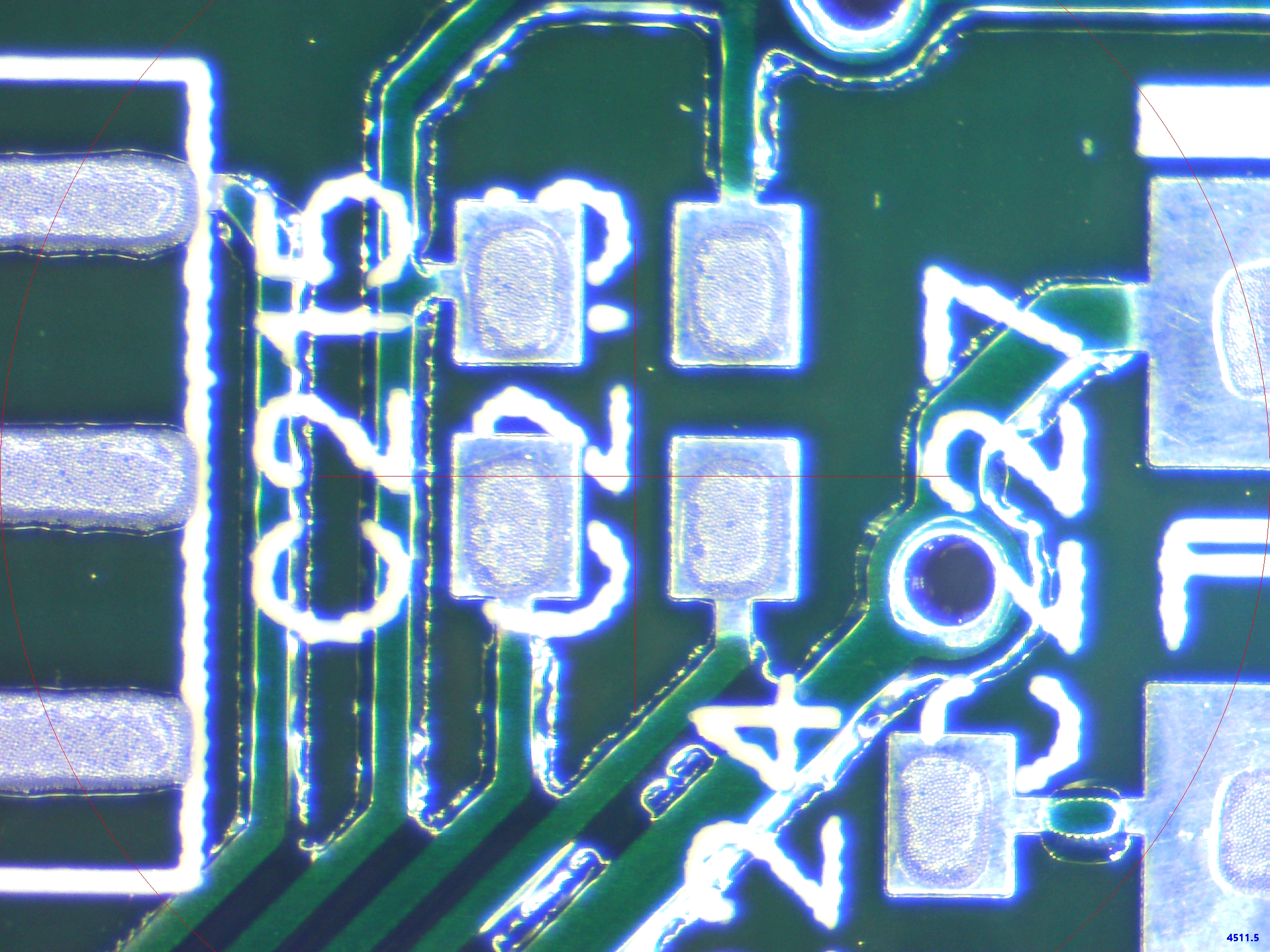
1320> Baking is complete. The micoUSB placed well but floated in the oven, C219 and C225 tombstoned. The MSPs look good.
1338> I am attempting to correct the microUSB, C219, and C225 using the soldering iron and hot air rework station.
1404> I wasn't able to move the microUSB, but I may have fixed C219 and C225 using a bit of solder paste and hot air at 350°F/10%.
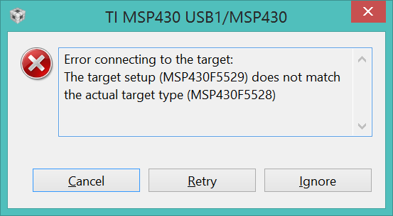
1408> I connected the JTAG probe to the 5529 first since there were no build errors with anything connected to it. The project is for the 5528, so the processor ID did not match, BUT IT IS SIGNS OF LIFE!
1410> I am single-stepping on the 5528! I have blinking lights!
The microUSB popped off with hot air and revealed the cause of the float: the pattern on the board is backwards! I don't know how I overlooked that during the paper build, that was a major screw-up. The part won't fit on the board because the 6MHz crystal blocks access to the port. I will need to rig some sort of jumper-wire contraption to a microUSB jack dangling from the board, or sacrifice a USB cable and try to solder wires directly to the board.
I spent quite a while trying to mount jumper wires to the bare microUSB pads, and had 3 of 5 when 2 of the 3 popped off. I will need a better idea. I moved on to final assembly and functional testing.
I was able to make Stencil #2 work, given enough patience and practice, and eventually I had a complete and functional board. Unfortunately, two design errors rendered the USB and motors unusable and require a new layout and new PCBs to continue. The new 0402 pattern with custom paste will be used for future designs, hopefully making the paste application more reliable and reducing the number of tombstoned components.
The page contains a lot of research into creating my own stencils, which would be useful in situations where I needed a new stencil for an existing board. This would have been nice while I was learning the proper paste parameters (or if I forgot to apply them). But cutting my own stencils is not worth the trouble when ordering new boards, especially when OSH Stencils will do it for under $20.