

Dec 19 2015
I downloaded and installed EagleCAD 7.5.0 using the "freeware" license. All my limited board design experience has been with the lesser-known DipTrace. Eagle is much more popular than DipTrace, while a full version of DipTrace is about half the cost of Eagle.
Update 2016/03/15: Novarm has now released DipTrace v3 and raised the price. The full version is now $1200, which makes it only slight cheaper than the equivalent version of EagleCAD. The hobbled versions are cheaper, down to a free version. I can upgrade from v2.3 to v3 for $224.00. I am evaluating v3.0 now...
Update 20160418: EagleCAD is 30% off through the end of April. The version that makes the most sense for me is the "Eagle Make Pro" at $450 ($315 with discount), although the limitations seem severe at only 4 signal layers and 160mm x 100mm (about 4x6"). The equivalent version to DipTrace Full ($1200) is Eagle Business Pro ($1640, $1150 with discount).
I have been using EagleCAD just to review the LaunchPad schematic. In this very limited experience, I am a bit surprised to find that DipTrace seems to be better than Eagle, even with all its quirks.
Gumstix publishes the schematics and layout of their Overo Tobi IO
board using Eagle. I
downloaded
the schematic and layout and saved them locally to
S:\Src\HQ\Dev\SB\Chip\gumstix\overo\tobi\ref\PCB30002-R3564\
I downloaded
EagleCAD
and installed it on VS12 (D:\CL\EagleCAD\070500). The installer does
not inspire much confidence: It unzipped everything into a local
directory on C: first (assuming there would be enough space), the
setup dialog was sized so that the installation folder and browse
button were not visible, and the installer complains if the full path
to the installation directory does not already exist. This also
created confusion about whether the installer would create its own
subdirectory. It did not, which was the correct choice. The freeware
license should be enough for me to simply open and examine the gumstix
files.
I opened the schematic using EagleCAD. My initial impression was that the schematic was clean and well organized. I should be able to copy/paste easily.
The board layout opened in EagleCAD without any problems. It was difficult to determine how many layers were in the board because EagleCAD seems to use the term "layer" to refer to organizational layers, showing 31 layers being used. The board can't have more than 4 physical layers.
This may be a chance to compare EagleCAD and DipTrace side-by-side. DipTrace was chosen by Lawrence, primarily based on cost and his past experience using it. The full version of DipTrace is about half the price of the equivalent version of Eagle. DipTrace has been adequate for the few and tiny projects I have done so far, but the persistent problem is that Eagle is far more popular than DipTrace and most projects that are open-sourced are published as Eagle projects.
Layout files are converted the same way, using the Eagle_to_DipTrace_BRD.ulp script.
The translation went smoothly, the only minor glitch I noticed (without actually trying to use the schematic) is that everything is offset to the upper left quadrant of the sheet and overflows the bounds. It seems Eagle puts the origin at the lower left corner of the sheet and DipTrace puts it in the center.
The board translation was a bit messier. It had the same offset problem, there were a lot of ratlines (indicating unrouted connections), and the board outline was a triangle rather than a rectangle (the final connection from point 4 back to point 1 missing?).
Looking at the board in DipTrace it seems to have 6 physical layers: Top, GND, S3, S14, Power, and Bottom. The GND layer seems to have nothing in it and the Power layer has exactly 1(!) short trace. A closer inspection of the DipTrace layout reveals some obvious import errors.
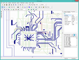
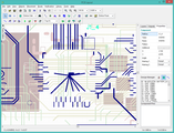
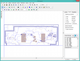
The first two screenshots show confusion around the two ICs, and the third shows all the unrouted ratlines. Eagle makes it difficult to match the layout components to the schematic parts as I can't click on the IC in the layout to see which component was used. The components are labelled IC6 and IC7 on the layout, and IC6 is labelled as "LAN" in the schematic. But IC7 is some mystery device with no name.
Comparing original Eagle layout with the DipTrace conversion around the area of the confused traces reveals the cause. The Eagle layout shows copper pours in the Top layer under the ICs with vias being used as connections to the GND plane. This technique would provide both an electrical connection to GND as well as a thermal sink into the large copper pour of the GND plane. DipTrace saw the vias but not the copper pours and did not make the connection to the GND plane, instead connected the vias with traces on the Top layer. I suspect the ratlines are a similar situation.
I am confused by the Eagle GND layer, as it seems to be completely empty. If it were an actual ground plane I would expect to see a huge copper pour filling the entire board. Aha! I disable all the layers except GND (View > Layers), selected the "info" mode, and right-clicked the faint outline in the GND layer. This brought up the object properties and I was able to then see that there is a giant copper pour assigned to the GND signal. This still leaves me wondering why I don't see the isolation wells around all the non-GND through vias, there seems to be no way to "fill in" the ground pour visually. I think DipTrace does a better job of visualizing the connections in layout. OK, the pours are filled when I click "Tools > Ratsnest". The GND layer was intentionally set to faint color, which can be changed by View > Layers > GND > Change > Color/Fillstyle.
I tried converting the Eagle layout again, this time clicking Tools > Ratsnest before exporting the ASCII file. The result was even worse. The GND pour was placed on the Top layer. I manually moved the GND and SHIELD pours to the GND layer, then updated them. The result was a hideous mess. Additional problems: the DRC rules were not imported so the DRC resulted in hundreds of errors; the copper pour was intersected with all the drill holes to create a very complex (and wrong) set of polygon corners.
If I were determined to convert the layout from Eagle to DipTrace, I would first remove all the copper pours from the Eagle layout. This will result in a large number of broken nets that will need to be reconnected after importing into DipTrace. Hopefully this would be a quick and simple step solved by recreating the pours in DipTrace. The conversion script simply does not handle the pours well at all.
Another look at the Power layer reveals another large copper pour. The lone trace in the Power layer was actually an isolated non-Power connection inside the pour.
I'm not sure this layout would be worth salvaging in DipTrace. If I were making a minor change to the existing Tobi layout, it would probably be quicker to learn EagleCAD than to fix it in DipTrace. However, my goal is not to rebuild the Tobi board as-is. The goal is to create and build a stripped-down version of the Tobi that I can then use as the foundation to build it back up into an MSP430-based motor control and sensor board.
DipTrace uses the right mouse button to pan, scroll wheel to zoom, and quickly becomes natural. Eagle uses the scroll wheel to zoom and hold the scroll wheel to pan. This is not nearly as natural as using the right button, but leaves the right button available for more standard functions. I am surprised that nobody seems to have played Darwinia, which has the most natural and efficient method for navigating a large space: zoom in and out while centering on the cursor. No dragging involved: just zoom out, move the cursor to the new location, and zoom back in. This completely eliminates the frustration of paddling across the universe and the awkwardness of trying to pan while holding a button down.
Both Eagle and DipTrace require pours to be updated manually. Eagle does this through the "Ratsnest" command, DipTrace does it by "updating" the object.