A couple general rules for board layout. These are guidelines, ranked more or less by priority.
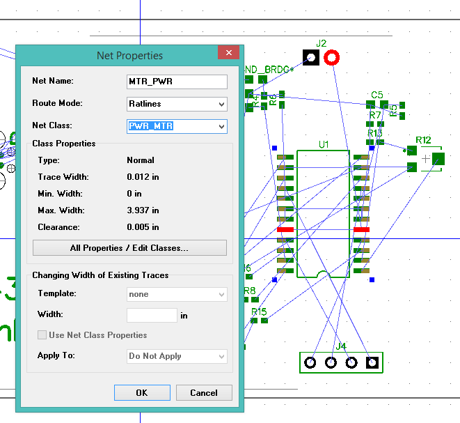
Taking the time to name the nets will eliminate a lot of confusion later. Every unique wire is a net. Place a component, right-click each pin, click "Net Properties" to open the dialog:
Set "Net Name" to any user-defined name, typically same as the pin name on the IC. It needs to be unique across the entire layout project; any pins connected to a net with the same name will be joined. For example, the net connected to the A3967 Reset pin should be named "A3967_RESET". On the other hand, all logic power pins should be connected to the same "Vcc" net.
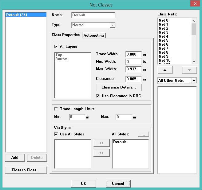
If this is a special connection, such as logic power or motor supply power, set the Net Class to one of my classes. If I need to define a new net class I can click the "All Properties / Edit Classes..." button.
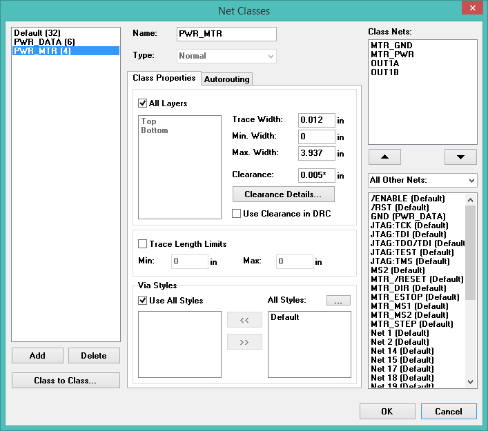
Here I can create a new net class and add nets to it. A net class allows me to specify non-standard trace width and design rules that will persist with the layout project. To create a new class I click the "Add" button, which will cause a new class to appear in the listbox. Make sure the proper class is selected before editing. type the name in "Name:", modify the class properties as needed, then add nets to the class using the selector on the right side.
Again, taking time to properly define the classes will save time and remove confusion later, especially if I need to create a new layout from scratch.
Unfortunately, DipTrace treats the trace width as a property of the layout pin when it really should be a property of the component pin. The component editor allows me to specify "Type" and "Electric" properties for each pin, but this seems to only be used for Spice analysis. I don't see how this information propagates to the layout phase. Plus, I it doesn't seem to be possible to add new values to either "Type" or "Electric"; I need to have (at least) two types of "Power" pins, digital power and motor supply power, each with specific trace widths and design rules. This means I need to recreate the net classes everytime I start a new layout, and manually assign the classes to each pin of every component I place.
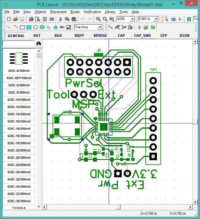
This is easy, simply create a new layout from the schematic. DipTrace will scatter the components around, then draw thin blue lines between the pads that need to be connected. This is the "ratlist" or rat's nest.
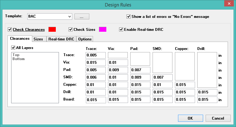
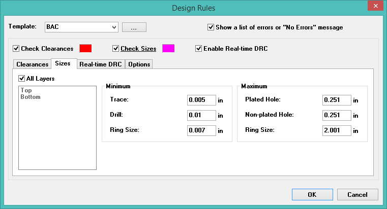
Before connecting anything, I need to know where the board will be sent for fabrication so that I know the design rules. Every board house will post their minimums on the website, such as minimum trace widths (usually 0.05" or 0.07"), minimum drill size (which dictates minimum via sizes, usually 0.10"), and so on. It is critical to set these design rules now, before investing any time in routing. Changing the minimum via size after routing will completely trash the layout. Try to minimize the number of hole sizes, this will affect the cost of fabrication.
It is a good idea to pad the design rules, if possible. Making the board smaller and more cramped than it needs to be will cause nothing but grief for a development board. However, the board will be dramatically easier to route if the design rules allow placing a trace between holes (0.10") and pads (0.5mm). This usually means using a trace/trace separation of 0.005", trace/pad separation of 0.005", trace/drill separation of 0.010", and trace/via separation of 0.015".
I need to set the default trace width. Most fabricators can go down to a minimum width of 0.005". Trust the posted minimums! If a fab house says that can make 0.005" traces, they can make 0.005" traces 100% of the time. There are a lot of factors that can go into determining the optimum trace width. I normally use 0.008" as this is the largest trace width that can pass between the posts of a 0.10" header row. The trace width is set by clicking Route > Route Setup...
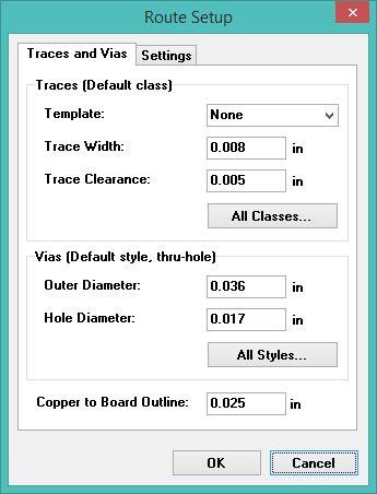
Design rules for Bay Area Circuits. Note that the trace/pad clearance is set to 0.005", which combined with a trace width of 0.008" allows traces to snake between the posts of a 0.10" header row. This is common practice and has been proven to be OK.
Let the machine do the first pass. It is much faster to tweak a bad solution than to start from scratch. Look for patterns in the layout. If the auto-router creates a layout with DRC violations that are impossible to fix, make sure to the "Use Clearance in DRC" option is set. This is buried in Route > Route Setup ... > Traces > All Classes ... NOTE: When I upgraded to v3beta, it seems this option is broken.
The auto-routing can always be improved, sometimes dramatically. Do not use static vias unless there is a compelling reason; create dynamic vias by simply switching layers (by pressing '1' or '2') while routing the wire. Be careful not to spend too much time tweaking. Don't make the board smaller and more cramped than it needs to be. Use vias as test points for signals.
Add silkscreen text for important notes, such as the location of +V/GND connections, Pin1 of bus connectors, revision ID, etc. Add mounting holes and at least two fiducials.
Fiducials are simply pads that expose copper without any connections. These are used to orient the Pick-n-Place machine over the board during assembly. Place a silkscreen crosshair around the fiducial to make it easier for the machine operator. Be sure to exclude the fiducial from the paste mask, to avoid dumping solder paste onto it. (Pattern Editor: Select fiducial pad > right-click > Mask/Paste Settings... > Disable for Pad > Top Paste Mask)
Stencil alignment holes are something Ron started using to help align the stencil over the board and to hold it in place while applying the solder paste. He found this to be necessary because I do not have a proper stencil printer table. Holding the stencil in place by hand or tape was allowing too much movement for the 0.5mm and 0.3mm fine pitch devices. Ron's tactic was to place a 0.126" unplated hole in each corner, then fit a 1/8" aluminum dowel into each hole through the stencil and board. He ran into some trouble with the dowels interfering with the path of the paste applicator, and with the holes being too tight. I will try 0.130" holes, which should only allow a maximum movement of less than 0.010", or 0.254mm. I can then minimize movement by manually squeezing the dowels to deform them into ellipsoids with a major chord greater than the nominal 0.125" to fill the hole more precisely.
Update: The stencil alignment holes are worthless. There is far too much slop between the hole, the stencil, and the rod. Aligning the stencil comes down to placing the stencil over the board and using my eyes to make sure it is aligned, then applying tape to hold the stencil in place. The alignment holes and rods do not help at all.
Make sure the stencil alignment holes are in the Top Paste (and
Bottom Paste if applicable) layers! The holes should appear in the Top
Paste gerber. I did this by creating a "PasteAlign" pattern, which
consists of three layers:
I also need to go back to the fine-pitch parts and modify the stencil layer so that the stencil apertures are slightly smaller than the solder mask. Through experience, I learned that for the very fine pitched pads it is better to have less solder than too much. A miniscule amount of solder on each of 24 pads will hold the IC in place.
I am still a bit confused about how DipTrace handles mask swell and paste shrink. Mask swell is the amount to expand the solder mask around the pad, paste shrink is the amount to contract the paste aperture within the pad. These two adjustments are used to make sure the pad is fully exposed but not overflowed with solder paste.
DipTrace allows me to set the mask swell and paste shrink values in three places: In the Pattern Editor I can select pad(s), right-click and select "Mask / Paste Settings..." to set custom settings for the pad. In the PCB Layout, I can also select pads and right-click "Mask / Paste Settings". And finally, when I export the Gerbers I can also set global Mask Swell and Paste Shrink values.
If I set the global mask swell and paste shrink to 0.0 in the Gerber export, this seems to override the values from the component pattern. Both the mask and the paste apertures are identical. This is not what I expect. Aha, I was selecting "update component" in PCB Layout. This updates the schematic component, not the pattern. I need to select "Replace Pattern" to update the pattern, being careful to select the same pattern from the library. Once I did this, my custom swell/shrink values for the component pattern were applied.
The physical constraints:
My working solution: For the fine-pitch components, set the mask swell to 0.0" and the paste shrink to 0.002". Leave the paste shrink at 0.0" for the mechanical mounting pads.
A subtle DipTrace bug: I adjust the swell/shrink values in the pattern library. I want to update the pattern in Layout, so I select the component, right-click "Replace Pattern". I want to select the same pattern again; I want to reload the updated pattern for the same component. I need to click on the library, then click on the part, then click OK -- even though I am not changing any selections. Otherwise, DipTrace does not actually update the pattern.
I am using GerberLogix to view the Gerber files output by DipTrace. GerberLogix is a simple but efficient viewer. It is highly recommended to use an independent Gerber viewer for the examination of the final Gerber output. [FILE 7050]